MAX3880ECB+D Maxim Integrated Products, MAX3880ECB+D Datasheet - Page 2
MAX3880ECB+D
Manufacturer Part Number
MAX3880ECB+D
Description
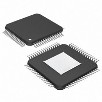
IC 1:16 DESERIALIZER 64-TQFP
Manufacturer
Maxim Integrated Products
Datasheet
1.MAX3880ECBD.pdf
(12 pages)
Specifications of MAX3880ECB+D
Function
Deserializer
Data Rate
2.5Gbps
Input Type
Serial
Output Type
LVDS
Number Of Inputs
1
Number Of Outputs
16
Voltage - Supply
3 V ~ 3.6 V
Operating Temperature
-40°C ~ 85°C
Mounting Type
Surface Mount
Package / Case
64-TQFP Exposed Pad, 64-eTQFP, 64-HTQFP, 64-VQFP
Lead Free Status / RoHS Status
Lead free / RoHS Compliant


ABSOLUTE MAXIMUM RATINGS
Positive Supply Voltage (V
Input Voltage Level (SDI+, SDI-, SLBI+, SLBI-,
Input Current Level (SDI+, SDI-, SLBI+, SLBI-)................±10mA
Voltage at LOL, SIS, PHADJ+, PHADJ-,
Output Current LVDS Outputs ............................................10mA
+3.3V, 2.488Gbps, SDH/SONET
1:16 Deserializer with Clock Recovery
DC ELECTRICAL CHARACTERISTICS
(V
V
Stresses beyond those listed under “Absolute Maximum Ratings” may cause permanent damage to the device. These are stress ratings only, and functional
operation of the device at these or any other conditions beyond those indicated in the operational sections of the specifications is not implied. Exposure to
absolute maximum rating conditions for extended periods may affect device reliability.
2
SERIAL DATA INPUTS (SDI±, SLBI±)
LVDS INPUTS AND OUTPUTS (SYNC±, PCLK±,
TTL INPUTS AND OUTPUTS (SIS, LOL)
CC
Supply Current
Differential Input Voltage
Single-Ended Input Voltage
Input Termination to Vcc
Input Voltage Range
Differential Input Threshold
Threshold Hysteresis
Differential Input Resistance
Output High Voltage
Output Low Voltage
Differential Output Voltage
Change in Magnitude of
Differential Output Voltage for
Complementary States
Output Offset Voltage
Change in Magnitude of Output
Offset Voltage for
Complementary States
Single-Ended Output
Resistance
Change in Magnitude of Single-
Ended Output Resistance for
Complementary Outputs
Input High Voltage
Input Low Voltage
Input Current
Output High Voltage
Output Low Voltage
SYNC+, SYNC-)........................... (V
FIL+, FIL- .................................................-0.5V to (V
CC
_______________________________________________________________________________________
= +3.3V, T
= +3.0V to +3.6V, differential loads = 100Ω ±1%, T
PARAMETER
A
= +25°C.)
CC
)...............................-0.5V to +7.0V
SYMBOL
∆|
CC
V
V
|
∆
∆
V
V
V
V
V
V
I
R
HYST
R
V
V
V
IDTH
R
V
V
V
CC
V
OH
OD
R
OH
OL
OS
OL
ID
IH
IS
IN
IN
IL
OD
O
OS
- 0.5V) to (V
I
O
|
|
Figure 1
Differential input voltage = 100mV
Common-mode voltage = 50mV
Figure 2
PD_±)
CC
CC
+ 0.5V)
+ 0.5V)
A
CONDITIONS
= -40°C to +85°C, unless otherwise noted. Typical values are at
Continuous Power Dissipation (T
Operating Temperature Range ...........................-40°C to +85°C
Storage Temperature Range .............................-55°C to +150°C
Lead Temperature (soldering, 10s) .................................+300°C
TQFP (derate 33.3mW/°C above +85°C) .......................1.44W
V
0.925
1.125
CC
-100
MIN
250
2.0
-10
2.4
50
85
40
0
- 0.4
A
= +85°C)
±2.5
TYP
275
100
50
78
95
V
CC
1.475
1.275
MAX
V
±25
±25
±10
+10
380
800
100
115
400
140
+ 0.2
2.4
0.8
0.4
CC
UNITS
mVp-p
mA
mV
mV
mV
mV
mV
µA
Ω
Ω
Ω
%
V
V
V
V
V
V
V
V
V
Related parts for MAX3880ECB+D
Image
Part Number
Description
Manufacturer
Datasheet
Request
R

Part Number:
Description:
MAX7528KCWPMaxim Integrated Products [CMOS Dual 8-Bit Buffered Multiplying DACs]
Manufacturer:
Maxim Integrated Products
Datasheet:
Part Number:
Description:
Single +5V, fully integrated, 1.25Gbps laser diode driver.
Manufacturer:
Maxim Integrated Products
Datasheet:
Part Number:
Description:
Single +5V, fully integrated, 155Mbps laser diode driver.
Manufacturer:
Maxim Integrated Products
Datasheet:
Part Number:
Description:
VRD11/VRD10, K8 Rev F 2/3/4-Phase PWM Controllers with Integrated Dual MOSFET Drivers
Manufacturer:
Maxim Integrated Products
Datasheet:
Part Number:
Description:
Highly Integrated Level 2 SMBus Battery Chargers
Manufacturer:
Maxim Integrated Products
Datasheet:
Part Number:
Description:
Current Monitor and Accumulator with Integrated Sense Resistor; ; Temperature Range: -40°C to +85°C
Manufacturer:
Maxim Integrated Products
Part Number:
Description:
TSSOP 14/A�/RS-485 Transceivers with Integrated 100O/120O Termination Resis
Manufacturer:
Maxim Integrated Products
Part Number:
Description:
TSSOP 14/A�/RS-485 Transceivers with Integrated 100O/120O Termination Resis
Manufacturer:
Maxim Integrated Products
Part Number:
Description:
QFN 16/A�/AC-DC and DC-DC Peak-Current-Mode Converters with Integrated Step
Manufacturer:
Maxim Integrated Products
Part Number:
Description:
TDFN/A/65V, 1A, 600KHZ, SYNCHRONOUS STEP-DOWN REGULATOR WITH INTEGRATED SWI
Manufacturer:
Maxim Integrated Products
Part Number:
Description:
Integrated Temperature Controller f
Manufacturer:
Maxim Integrated Products
Part Number:
Description:
SOT23-6/I�/45MHz to 650MHz, Integrated IF VCOs with Differential Output
Manufacturer:
Maxim Integrated Products
Part Number:
Description:
SOT23-6/I�/45MHz to 650MHz, Integrated IF VCOs with Differential Output
Manufacturer:
Maxim Integrated Products
Part Number:
Description:
EVALUATION KIT/2.4GHZ TO 2.5GHZ 802.11G/B RF TRANSCEIVER WITH INTEGRATED PA
Manufacturer:
Maxim Integrated Products
Part Number:
Description:
QFN/E/DUAL PCIE/SATA HIGH SPEED SWITCH WITH INTEGRATED BIAS RESISTOR
Manufacturer:
Maxim Integrated Products
Datasheet: