MAX3880ECB+D Maxim Integrated Products, MAX3880ECB+D Datasheet - Page 7
MAX3880ECB+D
Manufacturer Part Number
MAX3880ECB+D
Description
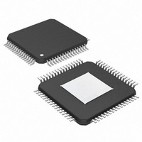
IC 1:16 DESERIALIZER 64-TQFP
Manufacturer
Maxim Integrated Products
Datasheet
1.MAX3880ECBD.pdf
(12 pages)
Specifications of MAX3880ECB+D
Function
Deserializer
Data Rate
2.5Gbps
Input Type
Serial
Output Type
LVDS
Number Of Inputs
1
Number Of Outputs
16
Voltage - Supply
3 V ~ 3.6 V
Operating Temperature
-40°C ~ 85°C
Mounting Type
Surface Mount
Package / Case
64-TQFP Exposed Pad, 64-eTQFP, 64-HTQFP, 64-VQFP
Lead Free Status / RoHS Status
Lead free / RoHS Compliant


dropped, shifting the alignment between PCLK and
data by 1 bit. The SYNC signal must be at least four
serial bit periods wide (4 x 402ps). See Figure 4 for the
timing diagram and Figure 5 for the timing parameters
diagram.
The input amplifiers on both the main data and system
loopback accept a differential input amplitude from
50mVp-p to 800mVp-p. The bit error rate (BER) is bet-
ter than 1 x 10
p, although the jitter tolerance performance will be
degraded. For interfacing with PECL signal levels, see
Applications Information.
The phase detector in the MAX3880 produces a volt-
age proportional to the phase difference between the
incoming data and the internal clock. Because of its
feedback nature, the PLL drives the error voltage to
zero, aligning the recovered clock to the center of the
incoming data eye for retiming. The external phase
adjust pins (PHADJ+, PHADJ-) allow the user to vary
the internal phase alignment.
The digital frequency detector (FD) aids frequency
acquisition during start-up conditions. The frequency
difference between the received data and the VCO
Figure 4. Timing Diagram
D15
TRANSMITTED FIRST
D14
D13
(MSB)
-10
(LSB) PD0
SYNC
PCLK
for input signals as small as 9.5mVp-
PD15
_______________________________________________________________________________________
PD1
SDI
•
•
•
1:16 Deserializer with Clock Recovery
Frequency Detector
D15
D0
D1
Phase Detector
Input Amplifier
+3.3V, 2.488Gbps, SDH/SONET
D16
D17
D31
clock is derived by sampling the in-phase and quadra-
ture VCO outputs on both edges of the data input sig-
nal. Depending on the polarity of the frequency
difference, the FD drives the VCO until the frequency
difference is reduced to zero. Once frequency acquisi-
tion is complete, the FD returns to a neutral state. False
locking is completely eliminated by this digital frequen-
cy detector.
The phase detector and frequency detector outputs are
summed into the loop filter. A 1.0µF capacitor, C
required to set the PLL damping ratio.
The loop filter output controls the on-chip LC VCO run-
ning at 2.488GHz. The VCO provides low phase noise
and is trimmed to the correct frequency.
A loss-of-lock (LOL) monitor is included in the
MAX3880 frequency detector. A loss-of-lock condition
is signaled immediately with a TTL low. When the PLL is
frequency-locked, LOL switches to TTL high in approxi-
mately 800ns.
Note that the LOL monitor is only valid when a data
stream is present on the inputs to the MAX3880. As a
result, LOL does not detect a loss-of-power condition
resulting from a loss of the incoming signal.
D32
D33
D47
1 BIT HAS SLIPPED
IN THIS TIME SLICE
D48
D49
D64
Loss-of-Lock Monitor
Loop Filter and VCO
D65
D66
D80
F
, is
7
Related parts for MAX3880ECB+D
Image
Part Number
Description
Manufacturer
Datasheet
Request
R

Part Number:
Description:
MAX7528KCWPMaxim Integrated Products [CMOS Dual 8-Bit Buffered Multiplying DACs]
Manufacturer:
Maxim Integrated Products
Datasheet:
Part Number:
Description:
Single +5V, fully integrated, 1.25Gbps laser diode driver.
Manufacturer:
Maxim Integrated Products
Datasheet:
Part Number:
Description:
Single +5V, fully integrated, 155Mbps laser diode driver.
Manufacturer:
Maxim Integrated Products
Datasheet:
Part Number:
Description:
VRD11/VRD10, K8 Rev F 2/3/4-Phase PWM Controllers with Integrated Dual MOSFET Drivers
Manufacturer:
Maxim Integrated Products
Datasheet:
Part Number:
Description:
Highly Integrated Level 2 SMBus Battery Chargers
Manufacturer:
Maxim Integrated Products
Datasheet:
Part Number:
Description:
Current Monitor and Accumulator with Integrated Sense Resistor; ; Temperature Range: -40°C to +85°C
Manufacturer:
Maxim Integrated Products
Part Number:
Description:
TSSOP 14/A�/RS-485 Transceivers with Integrated 100O/120O Termination Resis
Manufacturer:
Maxim Integrated Products
Part Number:
Description:
TSSOP 14/A�/RS-485 Transceivers with Integrated 100O/120O Termination Resis
Manufacturer:
Maxim Integrated Products
Part Number:
Description:
QFN 16/A�/AC-DC and DC-DC Peak-Current-Mode Converters with Integrated Step
Manufacturer:
Maxim Integrated Products
Part Number:
Description:
TDFN/A/65V, 1A, 600KHZ, SYNCHRONOUS STEP-DOWN REGULATOR WITH INTEGRATED SWI
Manufacturer:
Maxim Integrated Products
Part Number:
Description:
Integrated Temperature Controller f
Manufacturer:
Maxim Integrated Products
Part Number:
Description:
SOT23-6/I�/45MHz to 650MHz, Integrated IF VCOs with Differential Output
Manufacturer:
Maxim Integrated Products
Part Number:
Description:
SOT23-6/I�/45MHz to 650MHz, Integrated IF VCOs with Differential Output
Manufacturer:
Maxim Integrated Products
Part Number:
Description:
EVALUATION KIT/2.4GHZ TO 2.5GHZ 802.11G/B RF TRANSCEIVER WITH INTEGRATED PA
Manufacturer:
Maxim Integrated Products
Part Number:
Description:
QFN/E/DUAL PCIE/SATA HIGH SPEED SWITCH WITH INTEGRATED BIAS RESISTOR
Manufacturer:
Maxim Integrated Products
Datasheet: