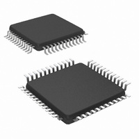
DS99R102VSX/NOPB National Semiconductor, DS99R102VSX/NOPB Datasheet - Page 18

DS99R102VSX/NOPB
Manufacturer Part Number
DS99R102VSX/NOPB
Description
IC DESERIALIZ 40MHZ 24BIT 48TQFP
Manufacturer
National Semiconductor
Datasheet
1.DS99R102VSNOPB.pdf
(24 pages)
Specifications of DS99R102VSX/NOPB
Function
Deserializer
Data Rate
960Mbps
Input Type
LVTTL/LVCMOS
Output Type
LVDS
Number Of Inputs
1
Number Of Outputs
24
Voltage - Supply
3 V ~ 3.6 V
Operating Temperature
0°C ~ 70°C
Mounting Type
Surface Mount
Package / Case
48-TQFP, 48-VQFP
Lead Free Status / RoHS Status
Lead free / RoHS Compliant
Other names
DS99R102VSX
Available stocks
Company
Part Number
Manufacturer
Quantity
Price
Company:
Part Number:
DS99R102VSX/NOPB
Manufacturer:
Texas Instruments
Quantity:
10 000
www.national.com
system with low-inductance parasitics, which has proven es-
pecially effective at high frequencies, and makes the value
and placement of external bypass capacitors less critical. Ex-
ternal bypass capacitors should include both RF ceramic and
tantalum electrolytic types. RF capacitors may use values in
the range of 0.01 uF to 0.1 uF. Tantalum capacitors may be
in the 2.2 uF to 10 uF range. Voltage rating of the tantalum
capacitors should be at least 5X the power supply voltage
being used.
Surface mount capacitors are recommended due to their
smaller parasitics. When using multiple capacitors per supply
pin, locate the smaller value closer to the pin. A large bulk
capacitor is recommend at the point of power entry. This is
typically in the 50uF to 100uF range and will smooth low fre-
quency switching noise. It is recommended to connect power
and ground pins directly to the power and ground planes with
bypass capacitors connected to the plane with via on both
ends of the capacitor. Connecting power or ground pins to an
external bypass capacitor will increase the inductance of the
path.
A small body size X7R chip capacitor, such as 0603, is rec-
ommended for external bypass. Its small body size reduces
the parasitic inductance of the capacitor. The user must pay
attention to the resonance frequency of these external bypass
capacitors, usually in the range of 20-30 MHz range. To pro-
vide effective bypassing, multiple capacitors are often used
to achieve low impedance between the supply rails over the
frequency of interest. At high frequency, it is also a common
practice to use two vias from power and ground pins to the
planes, reducing the impedance at high frequency.
Some devices provide separate power and ground pins for
different portions of the circuit. This is done to isolate switch-
ing noise effects between different sections of the circuit.
Separate planes on the PCB are typically not required. Pin
Description tables typically provide guidance on which circuit
blocks are connected to which power pin pairs. In some cas-
FIGURE 17. AC Coupled Application
18
es, an external filter many be used to provide clean power to
sensitive circuits such as PLLs.
Use at least a four layer board with a power and ground plane.
Locate LVCMOS (LVTTL) signals away from the LVDS lines
to prevent coupling from the LVCMOS lines to the LVDS lines.
Closely-coupled differential lines of 100 Ohms are typically
recommended for LVDS interconnect. The closely coupled
lines help to ensure that coupled noise will appear as com-
mon-mode and thus is rejected by the receivers. The tightly
coupled lines will also radiate less.
Termination of the LVDS interconnect is required. For point-
to-point applications, termination should be located at both
ends of the devices. Nominal value is 100 Ohms to match the
line’s differential impedance. Place the resistor as close to the
transmitter DOUT± outputs and receiver RIN± inputs as pos-
sible to minimize the resulting stub between the termination
resistor and device.
LVDS INTERCONNECT GUIDELINES
See AN-1108 and AN-905 for full details.
•
•
•
•
•
•
•
Additional general guidance can be found in the LVDS
Owner’s Manual - available in PDF format from the National
web site at: www.national.com/lvds
Use 100Ω coupled differential pairs
Use the S/2S/3S rule in spacings
—S = space between the pair
—2S = space between pairs
—3S = space to LVCMOS/LVTTL signal
Minimize the number of VIA
Use differential connectors when operating above
500Mbps line speed
Maintain balance of the traces
Minimize skew within the pair
Terminate as close to the TX outputs and RX inputs as
possible
20207918


