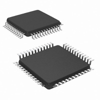
DS99R102VSX/NOPB National Semiconductor, DS99R102VSX/NOPB Datasheet

DS99R102VSX/NOPB
Specifications of DS99R102VSX/NOPB
Available stocks
Related parts for DS99R102VSX/NOPB
DS99R102VSX/NOPB Summary of contents
Page 1
... User selectable clock edge for parallel data on both Transmitter and Receiver Block Diagram TRI-STATE ® registered trademark of National Semiconductor Corporation. © 2007 National Semiconductor Corporation ■ Internal DC Balancing encode/decode – Supports AC- coupling interface with no external coding required ■ Individual power-down controls for both Transmitter and Receiver ■ ...
Page 2
... Absolute Maximum Ratings If Military/Aerospace specified devices are required, please contact the National Semiconductor Sales Office/ Distributors for availability and specifications. Supply Voltage ( LVCMOS/LVTTL Input Voltage LVCMOS/LVTTL Output Voltage LVDS Receiver Input Voltage LVDS Driver Output Voltage LVDS Output Short Circuit Duration ...
Page 3
Symbol Parameter V Output Differential Voltage OD (D )–(D ) OUT+ OUT− ΔV Output Differential Voltage OD Unbalance V Offset Voltage OS ΔV Offset Voltage Unbalance OS I Output Short Circuit Current OS I TRI-STATE Output Current OZ SER/DES SUPPLY ...
Page 4
Serializer Timing Requirements for TCLK Over recommended operating supply and temperature ranges unless otherwise specified. Symbol Parameter t Transmit Clock Period TCP t Transmit Clock High Time TCIH t Transmit Clock Low Time TCIL t TCLK Input Transition Time CLKT ...
Page 5
Symbol Parameter t ROUT (23:16) Setup Data to ROS RCLK (Group 3) t ROUT (23:16) Hold Data to ROH RCLK (Group 3) t HIGH to TRI-STATE Delay HZR t LOW to TRI-STATE Delay LZR t TRI-STATE to HIGH Delay ZHR ...
Page 6
AC Timing Diagrams and Test Circuits FIGURE 3. Serializer LVDS Output Load and Transition Times www.national.com FIGURE 1. Serializer Input Checker-board Pattern FIGURE 2. Deserializer Output Checker-board Pattern FIGURE 4. Serializer Input Clock Transition Times 6 20207902 20207903 20207904 20207906 ...
Page 7
FIGURE 5. Serializer Setup/Hold Times FIGURE 6. Serializer TRI-STATE Test Circuit and Delay 7 20207907 20207908 www.national.com ...
Page 8
FIGURE 7. Serializer PLL Lock Time, and TPWDNB TRI-STATE Delays FIGURE 9. Transmitter Output Eye Opening (TxOUT_E_O) www.national.com FIGURE 8. Serializer Delay 8 20207909 20207910 20207915 ...
Page 9
VOD = (D ) – OUT+ OUT - Differential output signal is shown – (D OUT+ FIGURE 11. Deserializer LVCMOS/LVTTL Output Load and Transition Times ), device in Data Transfer mode. OUT - FIGURE 10. ...
Page 10
Note: C includes instrumentation and fixture capacitance within ROUT[23:0] L FIGURE 13. Deserializer TRI-STATE Test Circuit and Timing FIGURE 14. Deserializer PLL Lock Times and RPWDNB TRI-STATE Delay www.national.com 20207913 10 20207914 ...
Page 11
RxIN_TOL_L is the ideal noise margin on the left of the figure, with respect to ideal. RxIN_TOL_R is the ideal noise margin on the right of the figure, with respect to ideal. FIGURE 16. Receiver Input Tolerance (RxIN_TOL) and Sampling ...
Page 12
DS99R101 Serializer Pin Descriptions Pin # Pin Name I/O LVCMOS PARALLEL INTERFACE PINS 4-1, DIN[23:0] LVCMOS_I 48-44, 41-32, 29-25 10 TCLK LVCMOS_I CONTROL AND CONFIGURATION PINS 9 TPWDNB LVCMOS_I 18 DEN LVCMOS_I 11 TRFB LVCMOS_I 12 VODSEL LVCMOS_I 5 DCAOFF ...
Page 13
DS99R101 Pin Diagram Serializer - DS99R101 TOP VIEW 13 20207919 www.national.com ...
Page 14
DS99R102 Deserializer Pin Descriptions Pin # Pin Name I/O LVCMOS PARALLEL INTERFACE PINS 25-28, ROUT[7:0] LVCMOS_O 31-34 13-16, ROUT[15:8] LVCMOS_O 21-24 3-6, ROUT[23:16] LVCMOS_O 9-12 18 RCLK LVCMOS_O CONTROL AND CONFIGURATION PINS 43 RRFB LVCMOS_I 48 REN LVCMOS_I 1 RPWDNB ...
Page 15
DS99R102 Pin Diagram Deserializer - DS99R102 TOP VIEW 15 20207920 www.national.com ...
Page 16
Functional Description The DS99R101 Serializer and DS99R102 Deserializer chipset is an easy-to-use transmitter and receiver pair that sends 24-bits of parallel LVCMOS data over a single serial LVDS link from 72 Mbps to 960 Mbps throughput. The DS99R101 transforms a ...
Page 17
LOCK pin to determine whether data on the ROUT is valid. POWERDOWN The Powerdown state is a low power sleep mode that the Se- rializer and Deserializer may use to reduce power when no data is being ...
Page 18
Ex- ternal bypass capacitors should include both RF ceramic and tantalum electrolytic types. RF capacitors ...
Page 19
FIGURE 18. DS99R101 Typical Application Connection 19 20207921 www.national.com ...
Page 20
FIGURE 19. DS99R102 Typical Application Connection www.national.com 20 20207922 ...
Page 21
Truth Tables TPWDNB (Pin 9) (Pin 18 RPWDNB REN (Pin 1) (Pin 48 TABLE 1. DS99R101 Serializer Truth Table DEN Tx PLL Status (Internal ...
Page 22
Physical Dimensions Ordering Information NSID DS99R101VS 48 Lead TQFP style, 7.0 X 7.0 X 1.0 mm, 0.5 mm pitch DS99R101VSX 48 Lead TQFP style, 7.0 X 7.0 X 1.0 mm, 0.5 mm pitch, 1000 std reel DS99R102VS 48 Lead TQFP ...
Page 23
Notes 23 www.national.com ...
Page 24
... National Semiconductor and the National Semiconductor logo are registered trademarks of National Semiconductor Corporation. All other brand or product names may be trademarks or registered trademarks of their respective holders. ...


