DS99R102VSX/NOPB National Semiconductor, DS99R102VSX/NOPB Datasheet - Page 14
DS99R102VSX/NOPB
Manufacturer Part Number
DS99R102VSX/NOPB
Description
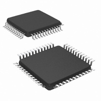
IC DESERIALIZ 40MHZ 24BIT 48TQFP
Manufacturer
National Semiconductor
Datasheet
1.DS99R102VSNOPB.pdf
(24 pages)
Specifications of DS99R102VSX/NOPB
Function
Deserializer
Data Rate
960Mbps
Input Type
LVTTL/LVCMOS
Output Type
LVDS
Number Of Inputs
1
Number Of Outputs
24
Voltage - Supply
3 V ~ 3.6 V
Operating Temperature
0°C ~ 70°C
Mounting Type
Surface Mount
Package / Case
48-TQFP, 48-VQFP
Lead Free Status / RoHS Status
Lead free / RoHS Compliant
Other names
DS99R102VSX
Available stocks
Company
Part Number
Manufacturer
Quantity
Price
Company:

Part Number:
DS99R102VSX/NOPB
Manufacturer:
Texas Instruments
Quantity:
10 000


www.national.com
LVCMOS PARALLEL INTERFACE PINS
25-28,
31-34
13-16,
21-24
3-6,
9-12
18
CONTROL AND CONFIGURATION PINS
43
48
1
17
2
LVDS SERIAL INTERFACE PINS
41
42
POWER / GROUND PINS
39
40
47
46
45
44
37
38
36
35
30
29
20
19
7
8
Pin #
DS99R102 Deserializer Pin Descriptions
ROUT[7:0]
ROUT[15:8]
ROUT[23:16] LVCMOS_O
RCLK
RRFB
REN
RPWDNB
LOCK
RESRVD
RIN+
RIN−
VDDIR
VSSIR
VDDPR0
VSSPR0
VDDPR1
VSSPR1
VDDR1
VSSR1
VDDR0
VSSR0
VDDOR1
VSSOR1
VDDOR2
VSSOR2
VDDOR3
VSSOR3
Pin Name
LVCMOS_O
LVCMOS_O
LVCMOS_O
LVCMOS_I
LVCMOS_I
LVCMOS_I
LVCMOS_O
LVCMOS_I
LVDS_I
LVDS_I
VDD
GND
VDD
GND
VDD
GND
VDD
GND
VDD
GND
VDD
GND
VDD
GND
VDD
GND
I/O
Receiver Parallel Interface Data Outputs – Group 1
Receiver Parallel Interface Data Outputs – Group 2
Receiver Parallel Interface Data Outputs – Group 3
Parallel Interface Clock Output Pin. Strobe edge set by RRFB configuration pin.
Receiver Clock Edge Select Pin
RRFB = H; ROUT LVCMOS Outputs strobed on the Rising Clock Edge.
RRFB = L; ROUT LVCMOS Outputs strobed on the Falling Clock Edge.
Receiver Data Enable
REN = H; ROUT[23-0] and RCLK are Enabled (ON).
REN = L; ROUT[23-0] and RCLK are Disabled (OFF), Receiver ROUT[23-0] and RCLK Outputs
are in TRI-STATE, PLL still operational and locked to TCLK.
Receiver Data Enable
REN = H; ROUT[23-0] and RCLK are Enabled (ON).
REN = L; ROUT[23-0] and RCLK are Disabled (OFF), Receiver ROUT[23-0] and RCLK Outputs
are in TRI-STATE, PLL still operational and locked to TCLK.
LOCK indicates the status of the receiver PLL
LOCK = H; receiver PLL is locked
LOCK = L; receiver PLL is unlocked, ROUT[23-0] and RCLK are TRI-STATED
RESERVED – This pin MUST be tied LOW.
Receiver LVDS True (+) Input This input is intended to be terminated with a 100 ohm load to
the RIN+ pin. The interconnect should be AC Coupled to this pin with a 100 nF capacitor.
Receiver LVDS Inverted (−) Input This input is intended to be terminated with a 100 ohm load
to the RIN- pin. The interconnect should be AC Coupled to this pin with a 100 nF capacitor.
Analog LVDS Voltage supply, Power
Analog LVDS Ground
Analog Voltage supply, PLL Power
Analog Ground, PLL Ground
Analog Voltage supply, PLL VCO Power
Analog Ground, PLL VCO Ground
Digital Voltage supply, Logic Power
Digital Ground, Logic Ground
Digital Voltage supply, Logic Power
Digital Ground, Logic Ground
Digital Voltage supply, LVCMOS Output Power
Digital Ground, LVCMOS Output Ground
Digital Voltage supply, LVCMOS Output Power
Digital Ground, LVCMOS Output Ground
Digital Voltage supply, LVCMOS Output Power
Digital Ground, LVCMOS Output Ground
14
Description
Related parts for DS99R102VSX/NOPB
Image
Part Number
Description
Manufacturer
Datasheet
Request
R

Part Number:
Description:
IC DESERIALIZ 40MHZ 24BIT 48TQFP
Manufacturer:
National Semiconductor
Datasheet:

Part Number:
Description:
National Semiconductor [8-Bit D/A Converter]
Manufacturer:
National Semiconductor
Datasheet:
Part Number:
Description:
National Semiconductor [Media Coprocessor]
Manufacturer:
National Semiconductor
Datasheet:
Part Number:
Description:
Digitally Controlled Tone and Volume Circuit with Stereo Audio Power Amplifier, Microphone Preamp Stage and National 3D Sound
Manufacturer:
National Semiconductor
Datasheet:
Part Number:
Description:
Digitally Controlled Tone and Volume Circuit with Stereo Audio Power Amplifier, Microphone Preamp Stage and National 3D Sound
Manufacturer:
National Semiconductor
Datasheet:
Part Number:
Description:
AC97 Rev 2 Codec with Sample Rate Conversion and National 3D Sound
Manufacturer:
National Semiconductor
Part Number:
Description:
Manufacturer:
National Semiconductor
Datasheet:
Part Number:
Description:
Manufacturer:
National Semiconductor
Datasheet:
Part Number:
Description:
General Purpose, Low Voltage, Low Power, Rail-to-Rail Output Operational Amplifiers
Manufacturer:
National Semiconductor
Datasheet:
Part Number:
Description:
8-bit 20 MSPS flash A/D converter.
Manufacturer:
National Semiconductor
Datasheet:
Part Number:
Description:
Low Noise Quad Operational Amplifier
Manufacturer:
National Semiconductor
Datasheet:
Part Number:
Description:
Quad Differential Line Receivers
Manufacturer:
National Semiconductor
Datasheet:
Part Number:
Description:
Quad High Speed Trapezoidal? Bus Transceiver
Manufacturer:
National Semiconductor
Datasheet:
Part Number:
Description:
Dual Line Receiver
Manufacturer:
National Semiconductor
Datasheet: