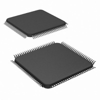
DS90CR485VS/NOPB National Semiconductor, DS90CR485VS/NOPB Datasheet - Page 7

DS90CR485VS/NOPB
Manufacturer Part Number
DS90CR485VS/NOPB
Description
IC SERIALIZER 48BIT 100-TQFP
Manufacturer
National Semiconductor
Datasheet
1.DS90CR485VSNOPB.pdf
(16 pages)
Specifications of DS90CR485VS/NOPB
Function
Serializer
Data Rate
6.384Gbps
Input Type
LVTTL/LVCMOS
Output Type
LVDS
Number Of Inputs
48
Number Of Outputs
8
Voltage - Supply
3.14 V ~ 3.46 V
Operating Temperature
-10°C ~ 70°C
Mounting Type
Surface Mount
Package / Case
100-TQFP, 100-VQFP
Number Of Elements
8
Number Of Receivers
48
Number Of Drivers
8
Operating Supply Voltage (typ)
2.5/3.3V
Differential Output Voltage
450mV
Power Dissipation
2.9W
Operating Temp Range
-10C to 70C
Operating Temperature Classification
Commercial
Mounting
Surface Mount
Pin Count
100
Package Type
TQFP
Leaded Process Compatible
Yes
Rohs Compliant
Yes
Peak Reflow Compatible (260 C)
Yes
For Use With
CLINK3V48BT-133 - BOARD EVAL FOR DS90CR485, 486
Lead Free Status / RoHS Status
Lead free / RoHS Compliant
Other names
*DS90CR485VS
*DS90CR485VS/NOPB
DS90CR485VS
*DS90CR485VS/NOPB
DS90CR485VS
Available stocks
Company
Part Number
Manufacturer
Quantity
Price
Company:
Part Number:
DS90CR485VS/NOPB
Manufacturer:
NSC
Quantity:
180
Company:
Part Number:
DS90CR485VS/NOPB
Manufacturer:
Texas Instruments
Quantity:
10 000
D0-D23
CLKIN
PD
TxOUTP
TxOUTM
CLK1P
CLK1M
PLLSEL
PRE
BAL
DS_OPT
TSEN
PRBS_EN
PAT_SEL
CON1
CON2
CON3
CON4
CON5 to
CON8
Pin Name
DS90CR485 Pin Description—Channel Link Serializer
I/O
O
O
O
O
O
I
I
I
I
I
I
I
I
I
I
I
I
I
I
No. of
Pins
24
1
1
8
8
1
1
1
1
1
1
1
1
1
1
1
1
1
4
LVCMOS/LVTTL level single-ended inputs. 3V tolerant when V
Note, external pull-down resistor of 1kΩ is required on all unused input data pins.
LVCMOS/LVTTL level clock input. Samples data on both edges. See Figure 5 and Figure 9.
3V tolerant when V
LVCMOS/LVTTL level input. PD = low activates the powerdown function and minimizes power
dissipation. 3V tolerant when V
Positive LVDS differential data output.
Negative LVDS differential data output.
Positive LVDS differential clock output.
Negative LVDS differential clock output.
LVCMOS/LVTTL level single-ended inputs. Control input for PLL range select. This pin must be
tied to V
3V tolerant when V
LVCMOS/LVTTL level single-ended inputs. Pre-emphasis level select. Pre-emphasis is active
when input is tied to V
pre-emphasis level (see table in application section). For normal LVDS levels (no pre-emphasis),
leave this pin open (do not tie to ground).
3V tolerant when V
LVCMOS/LVTTL level single-ended inputs. TTL level input. Tied this pin to Vcc to enable DC
Balance function. When tied low or left open, the DC Balance function is disabled. Please refer to
the Applications Information on the back for more information. See Figure 9 and Figure 10.
3V tolerant when V
LVCMOS/LVTTL level single-ended inputs. Cable Deskew performed when TTL level input is low.
No TxIN data is sampled during Deskew. To perform Deskew function, input must be held low for
a minimum of 4096 clock cycles. The Deskew operation is normally conducted after the TX and
RX PLLs have locked. It should also be conducted after a system reset, or a reconfiguration
event. Please refer to Applications Information section in back of this datasheet for more
information.
3V tolerant when V
Termination Sense pin. The logic state output of this pin reports the presence of a remote
termination resistor. TSEN is LOW when NO termination has been detected. TSEN is HIGH when
a termination of 100Ω has been detected.
Note, TSEN pin is an open-collector output, an external pull-up resistor of 1kΩ is required in order
for TSEN pin to function.
PRBS generator enable pin. The Pseudo Random Binary Sequence (PRBS) generator is enable
when this pin is tied High. Tie Low or float to disable the PRBS generator.
3V tolerant when V
PRBS-23 or PRBS-15 mode selection pin. PRBS-23 mode is enabled when this pin is tied High.
Tie Low or float to enable PRBS-15 mode.
3V tolerant when V
Control pin. This pin is reserved for future use. Tied to Low or NC.
Control pin. This pin must be tied High or pulled to high for normal operation Tied to Low for
internal BIST function only. Do not float.
3V tolerant when V
Control pin. This pin must be tied Low to configure the device for specific operation. Tied to
High or floating is reserved for future use.
Control pin. When tied High, all eight LVDS output channels (A0-A7) are enabled. Tied to Low will
disable LVDS output channels A4-A7. Must tie High for standard operation.
3V tolerant when V
Control pins. Tied to Low for normal operation.
CC
for 66MHz to 133 MHz operation. No connect or tied to low is reserved for future use.
CC3V
CC3V
CC3V
CC3V
CC3V
CC3V
CC3V
CC3V
CC3V
CC
= 3.3V.
= 3.3V. (Note 9)
= 3.3V.
= 3.3V.
= 3.3V.
= 3.3V.
= 3.3V.
= 3.3V.
= 3.3V.
through external pull-up resistor. Resistor value determines
CC3V
7
= 3.3V. (Note 9)
Description
CC3V
= 3.3V.
www.national.com


