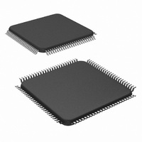
DS90CR485VS/NOPB National Semiconductor, DS90CR485VS/NOPB Datasheet - Page 2

DS90CR485VS/NOPB
Manufacturer Part Number
DS90CR485VS/NOPB
Description
IC SERIALIZER 48BIT 100-TQFP
Manufacturer
National Semiconductor
Datasheet
1.DS90CR485VSNOPB.pdf
(16 pages)
Specifications of DS90CR485VS/NOPB
Function
Serializer
Data Rate
6.384Gbps
Input Type
LVTTL/LVCMOS
Output Type
LVDS
Number Of Inputs
48
Number Of Outputs
8
Voltage - Supply
3.14 V ~ 3.46 V
Operating Temperature
-10°C ~ 70°C
Mounting Type
Surface Mount
Package / Case
100-TQFP, 100-VQFP
Number Of Elements
8
Number Of Receivers
48
Number Of Drivers
8
Operating Supply Voltage (typ)
2.5/3.3V
Differential Output Voltage
450mV
Power Dissipation
2.9W
Operating Temp Range
-10C to 70C
Operating Temperature Classification
Commercial
Mounting
Surface Mount
Pin Count
100
Package Type
TQFP
Leaded Process Compatible
Yes
Rohs Compliant
Yes
Peak Reflow Compatible (260 C)
Yes
For Use With
CLINK3V48BT-133 - BOARD EVAL FOR DS90CR485, 486
Lead Free Status / RoHS Status
Lead free / RoHS Compliant
Other names
*DS90CR485VS
*DS90CR485VS/NOPB
DS90CR485VS
*DS90CR485VS/NOPB
DS90CR485VS
Available stocks
Company
Part Number
Manufacturer
Quantity
Price
Company:
Part Number:
DS90CR485VS/NOPB
Manufacturer:
NSC
Quantity:
180
Company:
Part Number:
DS90CR485VS/NOPB
Manufacturer:
Texas Instruments
Quantity:
10 000
www.national.com
LVCMOS/LVTTL DC SPECIFICATIONS (All input pins.)
V
V
V
I
LVDS DC SPECIFICATIONS (All output pins TxOUTnP, TxOUTnM, CLKnP and CLKnM)
V
∆V
V
∆V
I
I
SUPPLY CURRENT
I
I
Symbol
IN
OS
OZ
CCTW
CCTZ
IH
IL
CL
OD
OS
Absolute Maximum Ratings
If Military/Aerospace specified devices are required,
please contact the National Semiconductor Sales Office/
Distributors for availability and specifications.
Electrical Characteristics
Over recommended operating supply and temperature ranges unless otherwise specified. (Note 2)
Supply Voltage (V
Supply Voltage (V
LVCMOS/LVTTL Input Voltage
LVDS Output Voltage
LVDS Short Circuit Duration
Maximum Package Power Dissipation
Lead Temperature
Junction Temperature
Storage Temperature Range
OD
OS
100 TQFP Package
Derate TQFP Package
(Soldering, 4 sec.)
High Level Input Voltage
Low Level Input Voltage
Input Clamp Voltage
Input Current
Differential Output Voltage
Change in V
Output States
Offset Voltage
Change in V
Output States
Output Short Circuit Current
Output TRI-STATE Current
2.5V Supply Current Worst Case
3.3V Supply Current Worst Case
Supply Current Power Down
CC
CC3
OD
OS
)
)
Parameter
Between Complimentary
Between Complimentary
23.8mW/˚C above +25˚C
−0.3V to (V
−0.3V to (V
@
−65˚C to +150˚C
25˚C
−0.2V to +2.7V
−0.3V to +3.6V
CC3
Continuous
CC
(Note 1)
+ 0.3V)
+ 0.3V)
+260˚C
+150˚C
I
V
V
R
V
PD = 0V, OUTM = OUTP = 0V or V
R
Worst Case Pattern,
100% Pre-emphasis
BAL = Low, Figure 1
R
Worst Case Pattern,
No Pre-emphasis
BAL = Low, Figure 1,
PD = Low
2.9W
CL
IN
IN
OUT
L
L
L
= 100Ω
= 100Ω, C
= 100Ω, C
= −18 mA
= 0.4V or V
= GND
= 0V, R
2
L
Recommended Operating
Conditions
L
L
ESD Rating:
Supply Voltage (V
Supply Voltage (V
Operating Free Air
Supply Noise Voltage
Clock Rate
Conditions
= 100Ω
CC
= 5 pF,
= 5 pF,
(HBM, 1.5kΩ, 100pF)
(EIAJ, 0Ω, 200pF)
Temperature (T
I/O and Control Pins
All Supply and GND pins
f = 66 MHz
f = 100 MHz
f = 133 MHz
A
CC
CC3
)
)
)
CC
2.37
2.37 2.5/3.3 3.46
Min
−10
GND
66
0.80
Min
−15
250
2.0
Nom
+25
2.5
1.125
−0.8
+1.8
−3.5
Typ
345
160
180
210
±
68
0
5
1
Max
2.62
+70
100
133
V
−1.5
Max
1.35
+15
−15
±
450
230
270
310
105
0.8
35
35
50
CC3
10
>
>
>
mV
Units
MHz
1.5kV
200V
˚C
2 kV
V
V
Units
p-p
mV
mV
mV
mA
mA
mA
mA
µA
µA
µA
µA
µA
V
V
V
V


