DS90CR485VS/NOPB National Semiconductor, DS90CR485VS/NOPB Datasheet - Page 3
DS90CR485VS/NOPB
Manufacturer Part Number
DS90CR485VS/NOPB
Description
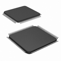
IC SERIALIZER 48BIT 100-TQFP
Manufacturer
National Semiconductor
Datasheet
1.DS90CR485VSNOPB.pdf
(16 pages)
Specifications of DS90CR485VS/NOPB
Function
Serializer
Data Rate
6.384Gbps
Input Type
LVTTL/LVCMOS
Output Type
LVDS
Number Of Inputs
48
Number Of Outputs
8
Voltage - Supply
3.14 V ~ 3.46 V
Operating Temperature
-10°C ~ 70°C
Mounting Type
Surface Mount
Package / Case
100-TQFP, 100-VQFP
Number Of Elements
8
Number Of Receivers
48
Number Of Drivers
8
Operating Supply Voltage (typ)
2.5/3.3V
Differential Output Voltage
450mV
Power Dissipation
2.9W
Operating Temp Range
-10C to 70C
Operating Temperature Classification
Commercial
Mounting
Surface Mount
Pin Count
100
Package Type
TQFP
Leaded Process Compatible
Yes
Rohs Compliant
Yes
Peak Reflow Compatible (260 C)
Yes
For Use With
CLINK3V48BT-133 - BOARD EVAL FOR DS90CR485, 486
Lead Free Status / RoHS Status
Lead free / RoHS Compliant
Other names
*DS90CR485VS
*DS90CR485VS/NOPB
DS90CR485VS
*DS90CR485VS/NOPB
DS90CR485VS
Available stocks
Company
Part Number
Manufacturer
Quantity
Price
Company:

Part Number:
DS90CR485VS/NOPB
Manufacturer:
NSC
Quantity:
180
Company:
Part Number:
DS90CR485VS/NOPB
Manufacturer:
Texas Instruments
Quantity:
10 000


TCIP
TCIH
TCIL
TCIT
TXIT
LLHT
LHLT
TCCS
TPPOS
TSTC
THTC
TJCC
BWPLL
TPLLS
TPDD
TPDL
Symbol
Symbol
Recommended Input Requirements
Over recommended operating supply and temperature ranges unless otherwise specified. (Note 2)
Switching Characteristics
Over recommended operating supply and temperature ranges unless otherwise specified. (Note 2)
Note 1: “Absolute Maximum Ratings” are those values beyond which the safety of the device cannot be guaranteed. They are not meant to imply that the device
should be operated at these limits. The tables of “Electrical Characteristics” specify conditions for device operation.
Note 2: Typical values are given for V
Note 3: LLHT and LHLT are measurements of transmitter LVDS data outputs rise and fall time over the recommended frequency range. The limits are based on
bench characterization and Guaranteed By Design (GBD) using statistical analysis.
Note 4: TPPOS is a measure of transmitter output pulse position in comparison with the ideal pulse position over the recommended frequency range. The limits are
based on bench characterization and Guaranteed By Design (GBD) using statistical analysis.
Note 5: TSTC and THTC are measurements of transmitter data inputs setup and hold time with clock input, CLKIN. The limits are based on bench characterization
and Guaranteed By Design (GBD) using statistical analysis.
Note 6: The limits are based on bench characterization of the device’s jitter response over the power supply voltage range. Output clock jitter is measured with a
cycle-to-cycle jitter of
without DC-Balance. The typical data is measured with a cycle-to-cycle jitter of
TxCLK IN Period (Figure 4)
TxCLK in High Time (Figure 4)
TxCLK in Low Time (Figure 4)
TxCLK IN Transition Time (Figure 3)
D0 to D23 Transition Time
LVDS Low-to-High Transition Time (No pre-emphasis, PRE = open) (Figure 2)
(Note 3)
LVDS Low-to-High Transition Time (max. pre-emphasis, PRE = V
(Note 3)
LVDS High-to-Low Transition Time (No pre-emphasis, PRE = open) (Figure 2)
(Note 3)
LVDS High-to-Low Transition Time (max. pre-emphasis, PRE = V
(Note 3)
TxOUT Channel-to-Channel Skew
Transmitter Output Pulse Position. (Note 4)
TxIN Setup to CLKIN at 133 MHz (Note 5), (Figure 5)
CLKIN to TxIN Hold at 133 MHz (Note 5), (Figure 5)
Transmitter Jitter Cycle-to-Cycle (Note 6)
PLL Bandwidth ≥ 66MHz
Transmitter Phase Lock Loop Set (Figure 6)
Transmitter Powerdown Delay (Figure 7)
Transmitter Input to Output Latency (Figure 8)
±
10% at a 1µs rate applied to the transmitter’s input clock signal (CLKIN) while data inputs are switching with internal PRBS generator enabled
CC
= 2.5V and T
Parameter
A
= +25˚C.
Parameter
±
3
100ps applied to the transmitter’s input clock signal (CLKIN).
f = 133 MHz
f = 100 MHz
f = 66 MHz
f = 133 MHz
f = 100 MHz
f = 66 MHz
CC
CC
) (Figure 2)
) (Figure 2)
133MHz
133MHz
66MHz
66MHz
6(TCIP)
−100
−150
−200
Min
0.5
0.5
0.35T
0.35T
7.52
Min
0.5
0.5
0.5
0.5
7(TCIP)
0.12
0.19
Typ
600
0.2
0.1
20
40
45
50
0.5T
0.5T
Typ
T
8(TCIP)
+ 200
+100
+150
Max
100
100
0.4
0.2
0.4
0.2
15.15
0.65T
0.65T
70
80
10
Max
1.75
www.national.com
2.4
1.2
2.9
Units
Units
kHz
ms
ns
ns
ns
ns
ns
ns
ns
ns
ns
ns
ns
ps
ps
ps
ps
ns
ns
ps
ps
ps
ns
ns
Related parts for DS90CR485VS/NOPB
Image
Part Number
Description
Manufacturer
Datasheet
Request
R

Part Number:
Description:
National Semiconductor [8-Bit D/A Converter]
Manufacturer:
National Semiconductor
Datasheet:
Part Number:
Description:
National Semiconductor [Media Coprocessor]
Manufacturer:
National Semiconductor
Datasheet:
Part Number:
Description:
Digitally Controlled Tone and Volume Circuit with Stereo Audio Power Amplifier, Microphone Preamp Stage and National 3D Sound
Manufacturer:
National Semiconductor
Datasheet:
Part Number:
Description:
Digitally Controlled Tone and Volume Circuit with Stereo Audio Power Amplifier, Microphone Preamp Stage and National 3D Sound
Manufacturer:
National Semiconductor
Datasheet:
Part Number:
Description:
AC97 Rev 2 Codec with Sample Rate Conversion and National 3D Sound
Manufacturer:
National Semiconductor
Part Number:
Description:
Manufacturer:
National Semiconductor
Datasheet:
Part Number:
Description:
Manufacturer:
National Semiconductor
Datasheet:
Part Number:
Description:
General Purpose, Low Voltage, Low Power, Rail-to-Rail Output Operational Amplifiers
Manufacturer:
National Semiconductor
Datasheet:
Part Number:
Description:
8-bit 20 MSPS flash A/D converter.
Manufacturer:
National Semiconductor
Datasheet:
Part Number:
Description:
Low Noise Quad Operational Amplifier
Manufacturer:
National Semiconductor
Datasheet:
Part Number:
Description:
Quad Differential Line Receivers
Manufacturer:
National Semiconductor
Datasheet:
Part Number:
Description:
Quad High Speed Trapezoidal? Bus Transceiver
Manufacturer:
National Semiconductor
Datasheet:
Part Number:
Description:
Dual Line Receiver
Manufacturer:
National Semiconductor
Datasheet:
Part Number:
Description:
TTL to 10k ECL Level Translator with Latch
Manufacturer:
National Semiconductor
Datasheet: