DS90CR485VS/NOPB National Semiconductor, DS90CR485VS/NOPB Datasheet - Page 11
DS90CR485VS/NOPB
Manufacturer Part Number
DS90CR485VS/NOPB
Description
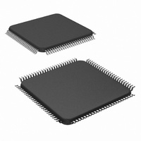
IC SERIALIZER 48BIT 100-TQFP
Manufacturer
National Semiconductor
Datasheet
1.DS90CR485VSNOPB.pdf
(16 pages)
Specifications of DS90CR485VS/NOPB
Function
Serializer
Data Rate
6.384Gbps
Input Type
LVTTL/LVCMOS
Output Type
LVDS
Number Of Inputs
48
Number Of Outputs
8
Voltage - Supply
3.14 V ~ 3.46 V
Operating Temperature
-10°C ~ 70°C
Mounting Type
Surface Mount
Package / Case
100-TQFP, 100-VQFP
Number Of Elements
8
Number Of Receivers
48
Number Of Drivers
8
Operating Supply Voltage (typ)
2.5/3.3V
Differential Output Voltage
450mV
Power Dissipation
2.9W
Operating Temp Range
-10C to 70C
Operating Temperature Classification
Commercial
Mounting
Surface Mount
Pin Count
100
Package Type
TQFP
Leaded Process Compatible
Yes
Rohs Compliant
Yes
Peak Reflow Compatible (260 C)
Yes
For Use With
CLINK3V48BT-133 - BOARD EVAL FOR DS90CR485, 486
Lead Free Status / RoHS Status
Lead free / RoHS Compliant
Other names
*DS90CR485VS
*DS90CR485VS/NOPB
DS90CR485VS
*DS90CR485VS/NOPB
DS90CR485VS
Available stocks
Company
Part Number
Manufacturer
Quantity
Price
Company:

Part Number:
DS90CR485VS/NOPB
Manufacturer:
NSC
Quantity:
180
Company:
Part Number:
DS90CR485VS/NOPB
Manufacturer:
Texas Instruments
Quantity:
10 000


Applications Information
PRE-EMPHASIS
Adds extra current during LVDS logic transition to reduce
cable loading effects. Pre-emphasis strength is set via a DC
voltage level applied from min to max (0.75V to V
“PRE” pin. A higher input voltage on the ”PRE” pin increases
the magnitude of dynamic current during data transition. The
INFORMATION ON JITTER REJECTION
The transmitter is designed to reject cycle-to-cycle jitter
which may be seen at the transmitter input clock. Very low
cycle-to-cycle jitter is passed on to the transmitter outputs.
Cycle-to-cycle jitter has been measured over frequency to
be less than 100ps with input step function jitter applied. This
significantly reduces the impact of input clock source jitter
and improves the accuracy of data sampling. Transmitter
output jitter is effected by PLLVCC noise and input clock jitter
- minimize supply noise and use a low jitter clock source to
limit output jitter.
DC BALANCE MODE
DC Balance mode is set when the BAL pin on the transmitter
and receiver are tied HIGH - see pin descriptions.
In addition to data information an additional bit is transmitted
on every LVDS data signal line during each cycle as shown
in Figure 10. This bit is the DC balance bit (BAL). The
TSEN
The TSEN pin reports the presence of a remote termination
resistor to the local system. The TSEN pin is an open-
collector output which requires an external pull-up resistor of
1kΩ at 2.5V to function. The logic state output of this pin
determines if there is termination on the far end of the LVDS
clock channel. When TSEN is High, a termination of 100Ω
has been detected. When TSEN is Low, no termination has
been detected indicating the likelihood that the cable is
unplugged. This pin reports the line status to the local sys-
tem.
BIST
To facilitate signal quality testing, an internal test pattern
generator is provided on chip. This can be useful in checking
signal quality (eye patterns) in the link. The internal BIST
BAL
0
1
1
1
1
1
Running Word Disparity
10kΩ or NC
Negative
Negative
Positive
Positive
TABLE 1. Pre-emphasis with (Rpre)
1.75KΩ
Zero
3.5kΩ
900Ω
500Ω
Rpre
50Ω
X
TABLE 2. DC Balance mode
CC
) at the
11
Current Word Disparity
“PRE” pin requires one pull-up resistor (Rpre) to V
to set the DC level. There is an internal resistor network,
which causes a voltage drop. Please refer to Table 1 on
value of Rpre to set the voltage level.
Depending upon interconnect performance and clock rate,
pre-emphasis, DC balance, and deskew enhancements al-
low cables 2 to 7 meters in length to be driven.
purpose of the DC Balance bit is to minimize the short- and
long-term DC bias on the signal lines. This is achieved by
selectively sending the data either unmodified or inverted.
The value of the DC balance bit is calculated from the
running word disparity and the data disparity of the current
word to be sent. The data disparity of the current word is
calculated by subtracting the number of bits of value 0 from
the number of bits value 1 in the current word. Initially, the
running word disparity may be any value between +7 and −6.
The running word disparity is the continuous sum of all the
modified data disparity values, where the unmodified data
disparity value is the calculated data disparity minus 1 if the
data is sent unmodified and 1 plus the inverse of the calcu-
lated data disparity if the data is sent inverted. The value of
the running word disparity saturates at +7 and −6 in DC
balance mode. Please refer to Table 2 for DC balance mode
operation.
function is activated by driving the PRBS_EN pin High.
There are two PRBS patterns available and the selections is
control by the logic state of the PAT_SEL pin. When PAT-
_SEL is High, the transmitter generate and send out a
PRBS-23 pattern. When PAT_SEL is low, a PRBS-15 pattern
will be generated and sent. When PRBS_EN pin is Low, the
logic state of the PAT_SEL pin will be ignored and the
transmitter will operate as indicated by the other control and
input pins. The transmitter’s internally generated PRBS pat-
terns are available for users to monitor signal quality via
eye-diagrams. Depending upon external test equipment re-
quirements, compatibility may or may not be possible.
12.5% pre-emphasis
100% pre-emphasis
25% pre-emphasis
50% pre-emphasis
75% pre-emphasis
Standard LVDS
Effects (Typ)
Negative/Zero
Negative/Zero
Positive
Positive
X
X
Data Sent Invert
YES
YES
YES
NO
NO
NO
www.national.com
CC
in order
Related parts for DS90CR485VS/NOPB
Image
Part Number
Description
Manufacturer
Datasheet
Request
R

Part Number:
Description:
National Semiconductor [8-Bit D/A Converter]
Manufacturer:
National Semiconductor
Datasheet:
Part Number:
Description:
National Semiconductor [Media Coprocessor]
Manufacturer:
National Semiconductor
Datasheet:
Part Number:
Description:
Digitally Controlled Tone and Volume Circuit with Stereo Audio Power Amplifier, Microphone Preamp Stage and National 3D Sound
Manufacturer:
National Semiconductor
Datasheet:
Part Number:
Description:
Digitally Controlled Tone and Volume Circuit with Stereo Audio Power Amplifier, Microphone Preamp Stage and National 3D Sound
Manufacturer:
National Semiconductor
Datasheet:
Part Number:
Description:
AC97 Rev 2 Codec with Sample Rate Conversion and National 3D Sound
Manufacturer:
National Semiconductor
Part Number:
Description:
Manufacturer:
National Semiconductor
Datasheet:
Part Number:
Description:
Manufacturer:
National Semiconductor
Datasheet:
Part Number:
Description:
General Purpose, Low Voltage, Low Power, Rail-to-Rail Output Operational Amplifiers
Manufacturer:
National Semiconductor
Datasheet:
Part Number:
Description:
8-bit 20 MSPS flash A/D converter.
Manufacturer:
National Semiconductor
Datasheet:
Part Number:
Description:
Low Noise Quad Operational Amplifier
Manufacturer:
National Semiconductor
Datasheet:
Part Number:
Description:
Quad Differential Line Receivers
Manufacturer:
National Semiconductor
Datasheet:
Part Number:
Description:
Quad High Speed Trapezoidal? Bus Transceiver
Manufacturer:
National Semiconductor
Datasheet:
Part Number:
Description:
Dual Line Receiver
Manufacturer:
National Semiconductor
Datasheet:
Part Number:
Description:
TTL to 10k ECL Level Translator with Latch
Manufacturer:
National Semiconductor
Datasheet: