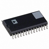
AD9814JRRL Analog Devices Inc, AD9814JRRL Datasheet - Page 2

AD9814JRRL
Manufacturer Part Number
AD9814JRRL
Description
IC CCD SIGNAL PROC 14BIT 28-SOIC
Manufacturer
Analog Devices Inc
Type
CCD Signal Processor, 14-Bitr
Specifications of AD9814JRRL
Rohs Status
RoHS non-compliant
Input Type
Logic
Output Type
Logic
Interface
3-Wire Serial
Current - Supply
80mA
Mounting Type
Surface Mount
Package / Case
28-SOIC (7.5mm Width)
Analog Front End Type
CCD
Analog Front End Category
Video
Interface Type
Serial (3-Wire)
Sample Rate
10MSPS
Operating Supply Voltage (min)
3/4.75V
Operating Supply Voltage (typ)
5V
Operating Supply Voltage (max)
5.25V
Resolution
14b
Supply Current
64/1.8mA
Number Of Adc's
1
Power Supply Type
Analog/Digital
Operating Temp Range
0C to 70C
Operating Temperature Classification
Commercial
Mounting
Surface Mount
Pin Count
28
Package Type
SOIC W
Number Of Channels
1
Lead Free Status / RoHS Status
Not Compliant
2 MHz, PGA Gain = 1, Input Range = 4 V, unless otherwise noted.)
AD9814–SPECIFICATIONS
ANALOG SPECIFICATIONS
Parameter
CONVERSION RATE
ACCURACY (Entire Signal Path)
ANALOG INPUTS
AMPLIFIERS
NOISE AND CROSSTALK
POWER SUPPLY REJECTION
Differential VREF (@ +25 C)
TEMPERATURE RANGE
POWER SUPPLIES
3-Channel Mode with CDS
1-Channel Mode with CDS
ADC Resolution
Integral Nonlinearity
Differential Nonlinearity (DNL)
No Missing Codes Guaranteed
Offset Error
Gain Error
Input Signal Range
Allowable Reset Transient
Input Limits
Input Capacitance
Input Bias Current
PGA Gain at Minimum
PGA Gain at Maximum
PGA Resolution
PGA Monotonicity
Programmable Offset at Minimum
Programmable Offset at Maximum
Programmable Offset Resolution
Programmable Offset Monotonicity
Input Referred Noise @ PGA Min
Total Output Noise @ PGA Min
Input Referred Noise @ PGA Max
Total Output Noise @ PGA Max
Channel-Channel Crosstalk
AVDD = +5 V
CAPT-CAPB (4 V Input Range)
CAPT-CAPB (2 V Input Range)
Operating
Storage
AVDD
DRVDD
Total Operating Current
Power-Down Mode Current
Power Dissipation
Power Dissipation @ 10 MHz
Power Dissipation (1-Channel Mode)
INL @ 10 MHz
DNL @ 10 MHz
AVDD
DRVDD
2
4
0.25 V
3
1
(INL)
3
(T
MIN
Min
13
AVSS – 0.3
0
–65
+4.75
+3.0
to T
MAX
, AVDD = +5 V, DRVDD = +5 V, 3-Channel CDS Mode, f
Guaranteed
Guaranteed
J-Grade
Typ
6
6
14
+2.5/–6.0
+4.0/–7.0
+0.6/–0.5
+0.8/–0.6
–12
2.2
4.0
1.0
10
10
1
5.8
64
–300
+300
512
130
0.55
84
2.0
<1
0.07
2.0
1.0
+5.0
+5.0
64
1.8
150
330
355
220
–2–
Max
10
7
AVDD + 0.3
+70
+150
+5.25
+5.25
Min
14
AVSS – 0.3
1.9
0.94
0
–65
+4.75
+3.0
Guaranteed
Guaranteed
K-Grade
Typ
6
6
14
+2.5/–6.0
+4.0/–7.0
+0.6/–0.5
+0.8/–0.6
–12
2.2
4.0
1.0
10
10
1
5.8
64
–300
+300
512
130
0.55
84
2.0
<1
0.07
2.0
1.0
+5.0
+5.0
64
1.8
150
330
355
220
ADCCLK
= 6 MHz, f
Max
10
7
AVDD + 0.3
0.3
2.1
1.06
+70
+150
+5.25
+5.25
80
10
450
265
11.0
1.0
104
5.3
CDSCLK1
= f
CDSCLK2
Units
Bits
LSB
LSB
LSB
LSB
mV
% FSR
V p-p
V
V
pF
V/V
V/V
LSB rms
LSB rms
% FSR
V
V
V
V
mA
mA
MSPS
MSPS
Bits
nA
Steps
mV
mV
Steps
LSB
mW
mW
mW
REV. 0
C
C
V rms
V rms
A
=


