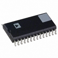
AD9814JRRL Analog Devices Inc, AD9814JRRL Datasheet

AD9814JRRL
Specifications of AD9814JRRL
Related parts for AD9814JRRL
AD9814JRRL Summary of contents
Page 1
FEATURES 14-Bit 10 MSPS A/D Converter No Missing Codes Guaranteed 3-Channel Operation MSPS 1-Channel Operation MSPS Correlated Double Sampling 1-6x Programmable Gain 300 mV Programmable Offset Input Clamp Circuitry Internal Voltage Reference Multiplexed ...
Page 2
AD9814–SPECIFICATIONS ANALOG SPECIFICATIONS 2 MHz, PGA Gain = 1, Input Range = 4 V, unless otherwise noted.) Parameter CONVERSION RATE 3-Channel Mode with CDS 1-Channel Mode with CDS ACCURACY (Entire Signal Path) ADC Resolution 1 Integral Nonlinearity (INL) INL @ ...
Page 3
NOTES 1 The Integral Nonlinearity in measured using the “fixed endpoint” method, NOT using a “best-fit” calculation. See Definitions of Specifications. 2 The Gain Error specification is dominated by the tolerance of the internal differential voltage reference. 3 Linear input ...
Page 4
AD9814 ABSOLUTE MAXIMUM RATINGS* With Respect Parameter To Min VIN, CAPT, CAPB AVSS –0.3 Digital Inputs AVSS –0.3 AVDD AVSS –0.5 DRVDD DRVSS –0.5 AVSS DRVSS –0.3 Digital Outputs DRVSS –0.3 Junction Temperature Storage Temperature –65 Lead Temperature (10 sec) ...
Page 5
DEFINITIONS OF SPECIFICATIONS INTEGRAL NONLINEARITY (INL) Integral nonlinearity error refers to the deviation of each indi- vidual code from a line drawn from “zero scale” through “posi- tive full scale.” The point used as “zero scale” occurs 1/2 LSB before ...
Page 6
AD9814 ANALOG t INPUTS CDSCLK1 t CDSCLK2 t ADCLK t ADCCLK t ADCLK OUTPUT DATA R (N–2) G (N–2) G (N–2) B (N–2) B (N–2) R (N–1) R (N–1) G (N–1) G (N–1) B (N–1) B (N–1) ...
Page 7
ANALOG INPUTS CDSCLK2 t ADCLK t ADCCLK t ADCLK OUTPUT DATA R (N–2) G (N–2) G (N–2) B (N–2) B (N–2) R (N–1) R (N–1) G (N–1) G (N–1) B (N–1) B (N–1) D<7:0> HIGH LOW BYTE BYTE ANALOG INPUTS ...
Page 8
AD9814 ADCCLK OUTPUT HIGH BYTE DATA DB13–DB6 <D7:D0> PIXEL N OEB R/Wb SDATA SCLK t LS SLOAD SDATA SCLK t LS SLOAD LOW LOW BYTE HIGH BYTE ...
Page 9
FUNCTIONAL DESCRIPTION The AD9814 can be operated in four different modes: 3-Channel CDS Mode, 3-Channel SHA Mode, 1-Channel CDS Mode, and 1-Channel SHA Mode. Each mode is selected by program- ming the Configuration Register through the serial interface. For more ...
Page 10
AD9814 INTERNAL REGISTER DESCRIPTIONS Register Address Name Configuration MUX Red PGA Green PGA Blue PGA Red Offset Green Offset ...
Page 11
PGA Gain Registers There are three PGA registers for individually programming the gain in the red, green and blue channels. Bits D8, D7 and D6 in each register must be set low, and bits D5 through D0 control the gain ...
Page 12
AD9814 CIRCUIT OPERATION Analog Inputs—CDS Mode Figure 8 shows the analog input configuration for the CDS mode of operation. Figure 9 shows the internal timing for the sampling switches. The CCD reference level is sampled when CDSCLK1 transitions from high ...
Page 13
Figure 12 shows how the OFFSET pin may be used in a CIS application for coarse offset adjustment. Many CIS signals have dc offsets ranging from several hundred millivolts to more than connecting the appropriate dc voltage ...
Page 14
AD9814 APPLICATIONS INFORMATION Circuit and Layout Recommendations The recommended circuit configuration for 3-Channel CDS mode operation is shown in Figure 15. The recommended input coupling capacitor value is 0.1 F (see Circuit Operation section for more details). A single ground ...
Page 15
PIN 1 0.0118 (0.30) 0.0040 (0.10) REV. 0 OUTLINE DIMENSIONS Dimensions shown in inches and (mm). 28-Lead, 300 Mil SOIC (R-28) 0.7125 (18.10) 0.6969 (17.70 0.2992 (7.60) 0.2914 (7.40) 0.4193 (10.65 0.3937 (10.00) 0.1043 (2.65) 0.0926 ...


