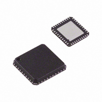
AD9949KCPZRL Analog Devices Inc, AD9949KCPZRL Datasheet - Page 7

AD9949KCPZRL
Manufacturer Part Number
AD9949KCPZRL
Description
IC CCD SIGNAL PROCESSOR 40-LFCSP
Manufacturer
Analog Devices Inc
Type
CCD Signal Processor, 12-Bitr
Datasheet
1.AD9949AKCPZ.pdf
(36 pages)
Specifications of AD9949KCPZRL
Input Type
Logic
Output Type
Logic
Interface
3-Wire Serial
Mounting Type
Surface Mount
Package / Case
40-LFCSP
Analog Front End Type
CCD
Analog Front End Category
Video
Interface Type
Serial (3-Wire)
Sample Rate
36MSPS
Input Voltage Range
0.5V
Operating Supply Voltage (min)
2.7V
Operating Supply Voltage (typ)
3V
Operating Supply Voltage (max)
3.6V
Resolution
12b
Number Of Adc's
1
Power Supply Type
Analog/Digital
Operating Temp Range
-20C to 85C
Operating Temperature Classification
Commercial
Mounting
Surface Mount
Pin Count
40
Package Type
LFCSP EP
Number Of Channels
1
Lead Free Status / RoHS Status
Lead free / RoHS Compliant
Current - Supply
-
Lead Free Status / RoHS Status
Compliant, Lead free / RoHS Compliant
Available stocks
Company
Part Number
Manufacturer
Quantity
Price
Company:
Part Number:
AD9949KCPZRL
Manufacturer:
PERICOM
Quantity:
3
PIN CONFIGURATION AND FUNCTION DESCRIPTIONS
Table 6. Pin Function Descriptions
Pin No.
1 to 4
5
6
7 to 13
14
15
16
17
18
19
20
21
22
23
24
25
26
27
28
29
30
31
32
33
34
35
36
37
38
39
40
1
Type: AI = Analog Input, AO = Analog Output, DI = Digital Input, DO = Digital Output, P = Power.
Mnemonic
D1 to D4
DRVSS
DRVDD
D5 to D11
H1
H2
HVSS
HVDD
H3
H4
RGVSS
RG
RGVDD
TCVSS
TCVDD
CLI
AVDD
CCDIN
AVSS
REFT
REFB
SL
SDI
SCK
VD
HD
DVSS
DVDD
HBLK
CLP/PBLK
D0
Type
DO
P
P
DO
DO
DO
P
P
DO
DO
P
DO
P
P
P
DI
P
AI
P
AO
AO
DI
DI
DI
DI
DI
P
P
DI
DO
DO
1
DRVDD
DRVSS
Description
Data Outputs
Digital Driver Ground
Digital Driver Supply
Data Outputs (D11 is MSB)
CCD Horizontal Clock 1
CCD Horizontal Clock 2
H1 to H4 Driver Ground
H1 to H4 Driver Supply
CCD Horizontal Clock 3
CCD Horizontal Clock 4
RG Driver Ground
CCD Reset Gate Clock
RG Driver Supply
Analog Ground for Timing Core
Analog Supply for Timing Core
Master Clock Input
Analog Supply for AFE
Analog Input for CCD Signal (Connect through Series 0.1 µF Capacitor)
Analog Ground for AFE
Reference Top Decoupling (Decouple with 1.0 µF to AVSS)
Reference Bottom Decoupling (Decouple with 1.0 µF to AVSS)
3-Wire Serial Load
3-Wire Serial Data Input
3-Wire Serial Clock
Vertical Sync Pulse
Horizontal Sync Pulse
Digital Ground
Digital Supply
Optional HBLK Input
CLPOB or PBLK Output
Data Output LSB
D1
D2
D3
D4
D5
D6
D7
D8
10
1
2
3
4
5
6
7
8
9
Figure 2. Pin Configuration
Rev. B | Page 7 of 36
PIN 1
INDICATOR
AD9949
TOP VIEW
30
29
28
27
26
25
24
23
22
21
REFB
REFT
AVSS
CCDIN
AVDD
CLI
TCVDD
TCVSS
RGVDD
RG
AD9949


