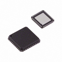
AD9949KCPZRL Analog Devices Inc, AD9949KCPZRL Datasheet - Page 3

AD9949KCPZRL
Manufacturer Part Number
AD9949KCPZRL
Description
IC CCD SIGNAL PROCESSOR 40-LFCSP
Manufacturer
Analog Devices Inc
Type
CCD Signal Processor, 12-Bitr
Datasheet
1.AD9949AKCPZ.pdf
(36 pages)
Specifications of AD9949KCPZRL
Input Type
Logic
Output Type
Logic
Interface
3-Wire Serial
Mounting Type
Surface Mount
Package / Case
40-LFCSP
Analog Front End Type
CCD
Analog Front End Category
Video
Interface Type
Serial (3-Wire)
Sample Rate
36MSPS
Input Voltage Range
0.5V
Operating Supply Voltage (min)
2.7V
Operating Supply Voltage (typ)
3V
Operating Supply Voltage (max)
3.6V
Resolution
12b
Number Of Adc's
1
Power Supply Type
Analog/Digital
Operating Temp Range
-20C to 85C
Operating Temperature Classification
Commercial
Mounting
Surface Mount
Pin Count
40
Package Type
LFCSP EP
Number Of Channels
1
Lead Free Status / RoHS Status
Lead free / RoHS Compliant
Current - Supply
-
Lead Free Status / RoHS Status
Compliant, Lead free / RoHS Compliant
Available stocks
Company
Part Number
Manufacturer
Quantity
Price
Company:
Part Number:
AD9949KCPZRL
Manufacturer:
PERICOM
Quantity:
3
SPECIFICATIONS
GENERAL SPECIFICATIONS
Table 1.
Parameter
TEMPERATURE RANGE
MAXIMUM CLOCK RATE
POWER SUPPLY VOLTAGE
POWER DISSIPATION
1
DIGITAL SPECIFICATIONS
T
Table 2.
Parameter
LOGIC INPUTS
LOGIC OUTPUTS
CLI INPUT
RG AND H-DRIVER OUTPUTS
The total power dissipated by the HVDD supply may be approximated using the equation
Total HVDD Power = (CLOAD x HVDD x Pixel Frequency) x HVDD x (Number of H – Outputs Used)
Reducing the H-loading, using only two of the outputs, and/or using a lower HVDD supply, reduces the power dissipation.
MIN
Operating
Storage
AVDD, TCVDD (AFE, Timing Core)
HVDD (H1 to H4 Drivers)
RGVDD (RG Driver)
DRVDD (D0 to D11 Drivers)
DVDD (All Other Digital)
36 MHz, HVDD = RGVDD = 3 V, 100 pF H1 to H4 Loading
Total Shutdown Mode
High Level Input Voltage
Low Level Input Voltage
High Level Input Current
Low Level Input Current
Input Capacitance
High Level Output Voltage, I
Low Level Output Voltage, I
High Level Input Voltage
Low Level Input Voltage
High Level Output Voltage
Low Level Output Voltage
Maximum Output Current (Programmable)
Maximum Load Capacitance
(TCVDD/2 + 0.5 V)
(RGVDD – 0.5 V and HVDD – 0.5 V)
to T
MAX
, AVDD = DVDD = DRVDD = HVDD = RGVDD = 2.7 V, C
OL
OH
= 2 mA
= 2 mA
1
Rev. B | Page 3 of 36
L
= 20 pF, unless otherwise noted.
Symbol
V
V
I
I
C
V
V
V
V
V
V
IH
IL
IH
IL
IN
OH
OL
IH–CLI
IL–CLI
OH
OL
Min
2.1
2.2
1.85
2.2
100
36
Min
−20
−65
2.7
2.7
2.7
2.7
2.7
Typ
3.0
3.0
3.0
3.0
3.0
320
1
Typ
10
10
10
30
Max
+85
+150
3.6
3.6
3.6
3.6
3.6
Max
0.6
0.5
0.85
0.5
AD9949
Unit
V
V
µA
µA
pF
V
V
V
V
V
V
mA
pF
Unit
°C
°C
MHz
V
V
V
V
V
mW
mW


