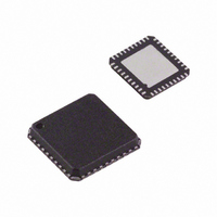
AD9949KCPZRL Analog Devices Inc, AD9949KCPZRL Datasheet - Page 6

AD9949KCPZRL
Manufacturer Part Number
AD9949KCPZRL
Description
IC CCD SIGNAL PROCESSOR 40-LFCSP
Manufacturer
Analog Devices Inc
Type
CCD Signal Processor, 12-Bitr
Datasheet
1.AD9949AKCPZ.pdf
(36 pages)
Specifications of AD9949KCPZRL
Input Type
Logic
Output Type
Logic
Interface
3-Wire Serial
Mounting Type
Surface Mount
Package / Case
40-LFCSP
Analog Front End Type
CCD
Analog Front End Category
Video
Interface Type
Serial (3-Wire)
Sample Rate
36MSPS
Input Voltage Range
0.5V
Operating Supply Voltage (min)
2.7V
Operating Supply Voltage (typ)
3V
Operating Supply Voltage (max)
3.6V
Resolution
12b
Number Of Adc's
1
Power Supply Type
Analog/Digital
Operating Temp Range
-20C to 85C
Operating Temperature Classification
Commercial
Mounting
Surface Mount
Pin Count
40
Package Type
LFCSP EP
Number Of Channels
1
Lead Free Status / RoHS Status
Lead free / RoHS Compliant
Current - Supply
-
Lead Free Status / RoHS Status
Compliant, Lead free / RoHS Compliant
Available stocks
Company
Part Number
Manufacturer
Quantity
Price
Company:
Part Number:
AD9949KCPZRL
Manufacturer:
PERICOM
Quantity:
3
AD9949
ABSOLUTE MAXIMUM RATINGS
Table 5.
Parameter
AVDD and TCVDD
HVDD and RGVDD
DVDD and DRVDD
Any VSS
Digital Outputs
CLPOB/PBLK and HBLK
SCK, SL, and SDATA
RG
H1 to H4
REFT, REFB, and CCDIN
Junction Temperature
Lead Temperature (10 s)
ESD CAUTION
ESD (electrostatic discharge) sensitive device. Electrostatic charges as high as 4000 V readily accumulate
on the human body and test equipment and can discharge without detection. Although this product features
proprietary ESD protection circuitry, permanent damage may occur on devices subjected to high energy elec-
trostatic discharges. Therefore, proper ESD precautions are recommended to avoid performance degradation
or loss of functionality.
With
Respect to
AVSS
HVSS,
RGVSS
DVSS,
DRVSS
Any VSS
DRVSS
DVSS
DVSS
RGVSS
HVSS
AVSS
Rating
−0.3 V to +3.9 V
−0.3 V to +3.9 V
−0.3 V to +3.9 V
−0.3 V to +0.3 V
−0.3 V to DRVDD + 0.3 V
−0.3 V to DVDD + 0.3 V
−0.3 V to DVDD + 0.3 V
−0.3 V to RGVDD + 0.3 V
−0.3 V to HVDD + 0.3 V
−0.3 V to AVDD + 0.3 V
150°C
300°C
Rev. B | Page 6 of 36
Stresses above those listed under Absolute Maximum Ratings
may cause permanent damage to the device. This is a stress
rating only; functional operation of the device at these or any
other conditions above those listed in the operational sections
of this specification is not implied. Exposure to absolute maxi-
mum rating conditions for extended periods may affect device
reliability.
THERMAL CHARACTERISTICS
Thermal Resistance
40-Lead LFCSP Package: θ
1
θ
board.
JA
is measured using a 4-layer PCB with the exposed paddle soldered to the
JA
= 27°C/W
1
.


