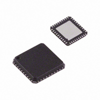
AD9949KCPZRL Analog Devices Inc, AD9949KCPZRL Datasheet - Page 19

AD9949KCPZRL
Manufacturer Part Number
AD9949KCPZRL
Description
IC CCD SIGNAL PROCESSOR 40-LFCSP
Manufacturer
Analog Devices Inc
Type
CCD Signal Processor, 12-Bitr
Datasheet
1.AD9949AKCPZ.pdf
(36 pages)
Specifications of AD9949KCPZRL
Input Type
Logic
Output Type
Logic
Interface
3-Wire Serial
Mounting Type
Surface Mount
Package / Case
40-LFCSP
Analog Front End Type
CCD
Analog Front End Category
Video
Interface Type
Serial (3-Wire)
Sample Rate
36MSPS
Input Voltage Range
0.5V
Operating Supply Voltage (min)
2.7V
Operating Supply Voltage (typ)
3V
Operating Supply Voltage (max)
3.6V
Resolution
12b
Number Of Adc's
1
Power Supply Type
Analog/Digital
Operating Temp Range
-20C to 85C
Operating Temperature Classification
Commercial
Mounting
Surface Mount
Pin Count
40
Package Type
LFCSP EP
Number Of Channels
1
Lead Free Status / RoHS Status
Lead free / RoHS Compliant
Current - Supply
-
Lead Free Status / RoHS Status
Compliant, Lead free / RoHS Compliant
Available stocks
Company
Part Number
Manufacturer
Quantity
Price
Company:
Part Number:
AD9949KCPZRL
Manufacturer:
PERICOM
Quantity:
3
Table 16. H1CONTROL, RGCONTROL, DRVCONTROL, and SAMPCONTROL Register Parameters
Parameter
Polarity
Positive Edge
Negative Edge
Sample Location
Drive Control
DOUT Phase
Table 17. Precision Timing Edge Locations
Quadrant
I
II
III
IV
H-DRIVER AND RG OUTPUTS
In addition to the programmable timing positions, the AD9949 features on-chip output drivers for the RG and H1 to H4 outputs. These
drivers are powerful enough to directly drive the CCD inputs. The H-driver and RG driver current can be adjusted for optimum rise/fall
time into a particular load by using the DRVCONTROL register (Address 0×62). The DRVCONTROL register is divided into five differ-
ent 3-bit values, each one being adjustable in 4.1 mA increments. The minimum setting of 0 is equal to OFF or three-state, and the maxi-
mum setting of 7 is equal to 30.1 mA.
As shown in Figure 18, the H2/H4 outputs are inverses of H1/H3. The internal propagation delay resulting from the signal inversion is
less than l ns, which is significantly less than the typical rise time driving the CCD load. This results in a H1/H2 crossover voltage at ap-
proximately 50% of the output swing. The crossover voltage is not programmable.
DIGITAL DATA OUTPUTS
The AD9949 data output phase is programmable using the DOUTPHASE register (Address 0×64). Any edge from 0 to 47 may be pro-
grammed, as shown in Figure 19. The pipeline delay for the digital data output is shown in Figure 20.
Edge Location (Decimal)
0 to 11
12 to 23
24 to 35
36 to 47
H1/H3
H2/H4
Length
1b
6b
6b
6b
3b
6b
Range
High/Low
0 to 47 Edge Location
0 to 47 Edge Location
0 to 47 Sample Location
0 to 7 Current Steps
0 to 47 Edge Location
t
RISE
FIXED CROSSOVER VOLTAGE
Figure 18. H-Clock Inverse Phase Relationship
t
PD
<<
Rev. B | Page 19 of 36
t
Register Value (Decimal)
0 to 11
16 to 27
32 to 43
48 to 59
RISE
Description
Polarity Control for H1/H3 and RG (0 = No Inversion, 1 = Inversion).
Positive Edge Location for H1/H3 and RG.
Negative Edge Location for H1/H3 and RG.
Sampling Location for SHP and SHD.
Drive Current for H1 to H4 and RG Outputs, 0 to 7 Steps of 4.1 mA Each.
Phase Location of Data Outputs with Respect to Pixel Period.
H1/H3
t
PD
Register Value (Binary)
000000 to 001011
010000 to 011011
100000 to 101011
110000 to 111011
H2/H4
AD9949


