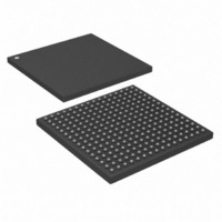
DS26514GN+ Maxim Integrated Products, DS26514GN+ Datasheet - Page 237

DS26514GN+
Manufacturer Part Number
DS26514GN+
Description
IC TXRX T1/E1/J1 4PORT 256-CSBGA
Manufacturer
Maxim Integrated Products
Type
Transceiverr
Datasheet
1.DS26514GN.pdf
(305 pages)
Specifications of DS26514GN+
Number Of Drivers/receivers
4/4
Protocol
Ethernet
Voltage - Supply
3.14 V ~ 3.47 V
Mounting Type
Surface Mount
Package / Case
256-CSBGA
Lead Free Status / RoHS Status
Lead free / RoHS Compliant
- Current page: 237 of 305
- Download datasheet (2Mb)
Register Name:
Register Description:
Register Addresses:
Bit #
Name
Default
Bit 6: Receive Hitless Protection Mode (RHPM).
If the TXENABLE pin is low and this bit is set to one, the receive LIU will present a high impedance to the line,
overriding the receive impedance selection register bits LRISMR.RIMPM[2:0].
Bits 5 and 4 : Jitter Attenuator Depth Select (JADS[1:0])
Bits 3 and 2: Jitter Attenuator Position Select (JAPS[1:0]). These bits are used to select the position of the jitter
attenuator.
Bit 1: T1J1E1 Selection (T1J1E1S). This bit configures the LIU for E1 or T1/J1 operation.
Bit 0: LOS Selection Criteria (LSC). This bit is used for LIU LOS selection criteria.
Rev: 101608
JADS1
JAPS1
0
0
1
1
0
0
1
1
0 = Normal operation using software for hitless protection (RIMPON).
1 = Hitless protection switching mode using TXENABLE pin.
0 = E1
1 = T1 or J1
E1 Mode
0 = G.775
1 = ETS 300 233
T1/J1 Mode
0 = T1.231
1 = T1.231
JADS0
JAPS0
—
7
0
0
1
0
1
0
1
0
1
Jitter attenuator FIFO depth 128 bits.
Jitter attenuator FIFO depth 64 bits.
Jitter attenuator FIFO depth 32 bits.
Jitter attenuator FIFO depth 16 bits (used for delay sensitive applications).
Jitter attenuator in the receive path.
Jitter attenuator in the transmit path.
Jitter attenuator disabled.
Jitter attenuator disabled.
LTRCR
LIU Transmit Receive Control Register
1000h + (20h x (n - 1)) : where n = 1 to 4
RHPM
6
0
FUNCTION
JADS1
5
0
JADS0
4
0
FUNCTION
JAPS1
3
0
DS26514 4-Port T1/E1/J1 Transceiver
JAPS0
2
0
T1J1E1S
1
0
237 of 305
LSC
0
0
Related parts for DS26514GN+
Image
Part Number
Description
Manufacturer
Datasheet
Request
R

Part Number:
Description:
4-port T1/e1/j1 Transceiver
Manufacturer:
Maxim Integrated Products, Inc.
Datasheet:

Part Number:
Description:
power light source LUXEON® Collimator
Manufacturer:
LUMILEDS [Lumileds Lighting Company]
Datasheet:

Part Number:
Description:
MAX7528KCWPMaxim Integrated Products [CMOS Dual 8-Bit Buffered Multiplying DACs]
Manufacturer:
Maxim Integrated Products
Datasheet:

Part Number:
Description:
Single +5V, fully integrated, 1.25Gbps laser diode driver.
Manufacturer:
Maxim Integrated Products
Datasheet:

Part Number:
Description:
Single +5V, fully integrated, 155Mbps laser diode driver.
Manufacturer:
Maxim Integrated Products
Datasheet:

Part Number:
Description:
VRD11/VRD10, K8 Rev F 2/3/4-Phase PWM Controllers with Integrated Dual MOSFET Drivers
Manufacturer:
Maxim Integrated Products
Datasheet:

Part Number:
Description:
Highly Integrated Level 2 SMBus Battery Chargers
Manufacturer:
Maxim Integrated Products
Datasheet:

Part Number:
Description:
Current Monitor and Accumulator with Integrated Sense Resistor; ; Temperature Range: -40°C to +85°C
Manufacturer:
Maxim Integrated Products

Part Number:
Description:
TSSOP 14/A°/RS-485 Transceivers with Integrated 100O/120O Termination Resis
Manufacturer:
Maxim Integrated Products

Part Number:
Description:
TSSOP 14/A°/RS-485 Transceivers with Integrated 100O/120O Termination Resis
Manufacturer:
Maxim Integrated Products

Part Number:
Description:
QFN 16/A°/AC-DC and DC-DC Peak-Current-Mode Converters with Integrated Step
Manufacturer:
Maxim Integrated Products

Part Number:
Description:
TDFN/A/65V, 1A, 600KHZ, SYNCHRONOUS STEP-DOWN REGULATOR WITH INTEGRATED SWI
Manufacturer:
Maxim Integrated Products

Part Number:
Description:
Integrated Temperature Controller f
Manufacturer:
Maxim Integrated Products

Part Number:
Description:
SOT23-6/I°/45MHz to 650MHz, Integrated IF VCOs with Differential Output
Manufacturer:
Maxim Integrated Products


