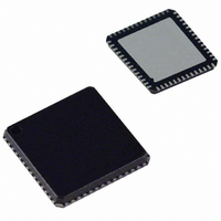
AD9911BCPZ Analog Devices Inc, AD9911BCPZ Datasheet - Page 7

AD9911BCPZ
Manufacturer Part Number
AD9911BCPZ
Description
IC DDS 500MSPS DAC 10BIT 56LFCSP
Manufacturer
Analog Devices Inc
Datasheet
1.AD9911BCPZ-REEL7.pdf
(44 pages)
Specifications of AD9911BCPZ
Resolution (bits)
10 b
Master Fclk
500MHz
Tuning Word Width (bits)
32 b
Voltage - Supply
1.71 V ~ 1.96 V
Operating Temperature
-40°C ~ 85°C
Mounting Type
Surface Mount
Package / Case
56-LFCSP
Transmitting Current
73mA
Data Rate
800Mbps
Rf Ic Case Style
LFCSP
No. Of Pins
56
Supply Voltage Range
1.71V To 1.89V, 3.135V To 3.465V
Operating Temperature Range
-40°C To +85°C
Msl
MSL 3 - 168 Hours
Lead Free Status / RoHS Status
Lead free / RoHS Compliant
For Use With
AD9911/PCBZ - BOARD EVAL FOR AD9911AD9911/PCB - BOARD EVAL FOR AD9911
Lead Free Status / Rohs Status
Compliant
Available stocks
Company
Part Number
Manufacturer
Quantity
Price
Company:
Part Number:
AD9911BCPZ
Manufacturer:
NXP
Quantity:
173
Part Number:
AD9911BCPZ
Manufacturer:
ADI/亚德诺
Quantity:
20 000
Parameter
I/O PORT TIMING CHARACTERISTICS
MISCELLANEOUS TIMING CHARACTERISTICS
CMOS LOGIC INPUT
CMOS LOGIC OUTPUTS (1 mA Load)
POWER SUPPLY
Maximum Frequency Clock (SCLK)
Minimum SCLK Pulse Width Low (t
Minimum SCLK Pulse Width High (t
Minimum Data Set-Up Time (t
Minimum Data Hold Time
Minimum CSB Set-Up Time (t
Master_Reset Minimum Pulse Width
I/O_Update Minimum Pulse Width
Minimum Set-Up Time (I/O_Update to
Minimum Hold Time (I/O_Update to
Minimum Set-Up Time (Profile Inputs to
Minimum Hold Time (Profile Inputs to
Minimum Set-Up Time (SDIO Inputs to
Minimum Hold Time (SDIO Inputs to
Propagation Delay Between REF_CLK and
V
V
Logic 1 Current
Logic 0 Current
Input Capacitance
V
V
Total Power Dissipation—Single-Tone Mode
Total Power Dissipation—With Sweep
Total Power Dissipation—3 Spur
Total Power Dissipation—Test-Tone
Total Power Dissipation—Full Power Down
IAVDD—Single-Tone Mode
IAVDD— Sweep Accumulator, REF_CLK
IDVDD—Single-Tone Mode
IDVDD—Sweep Accumulator, REF_CLK
IDVDD_I/O
IDVDD_I/O
IAVDD Power-Down Mode
IDVDD Power-Down Mode
Minimum Data Valid Time for Read Operation
IH
IL
OH
OL
Accumulator
Reduction/Multitone Channels Active
Modulation
Multiplier, and 10-Bit Output Scalar Enabled
Multiplier, and 10-Bit Output Scalar Enabled
SYNC_CLK)
SYNC_CLK)
SYNC_CLK)
SYNC_CLK)
SYNC_CLK)
SYNC_CLK)
SYNC_CLK
PRE
DS
)
)
PWL
PWH
)
)
Min
1.6
2.2
2.2
0
1.0
12
1
1
4.8
0
5.4
0
2.5
0
2.25
2.0
2.7
Rev. 0 | Page 7 of 44
Typ
3.5
3
−12
2
241
241
351
264
1.8
73
73
50
50
40
30
0.7
1.1
Max
200
5.5
0.8
12
0.4
Unit
MHz
ns
ns
ns
ns
ns
ns
ns
ns
ns
ns
ns
ns
ns
V
V
μA
μA
pF
V
V
mW
mW
mW
mW
mW
mA
mA
mA
mA
mA
mA
mA
mA
Test Conditions/Comments
Minimum pulse width = 1 sync clock period
Minimum pulse width = 1 sync clock period
Rising edge to rising edge
Rising edge to rising edge
Dominated by supply variation
Dominated by supply variation
Dominated by supply variation
Dominated by supply variation
IDVDD = read
IDVDD = write
AD9911


