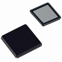
AD9911BCPZ Analog Devices Inc, AD9911BCPZ Datasheet - Page 29

AD9911BCPZ
Manufacturer Part Number
AD9911BCPZ
Description
IC DDS 500MSPS DAC 10BIT 56LFCSP
Manufacturer
Analog Devices Inc
Datasheet
1.AD9911BCPZ-REEL7.pdf
(44 pages)
Specifications of AD9911BCPZ
Resolution (bits)
10 b
Master Fclk
500MHz
Tuning Word Width (bits)
32 b
Voltage - Supply
1.71 V ~ 1.96 V
Operating Temperature
-40°C ~ 85°C
Mounting Type
Surface Mount
Package / Case
56-LFCSP
Transmitting Current
73mA
Data Rate
800Mbps
Rf Ic Case Style
LFCSP
No. Of Pins
56
Supply Voltage Range
1.71V To 1.89V, 3.135V To 3.465V
Operating Temperature Range
-40°C To +85°C
Msl
MSL 3 - 168 Hours
Lead Free Status / RoHS Status
Lead free / RoHS Compliant
For Use With
AD9911/PCBZ - BOARD EVAL FOR AD9911AD9911/PCB - BOARD EVAL FOR AD9911
Lead Free Status / Rohs Status
Compliant
Available stocks
Company
Part Number
Manufacturer
Quantity
Price
Company:
Part Number:
AD9911BCPZ
Manufacturer:
NXP
Quantity:
173
Part Number:
AD9911BCPZ
Manufacturer:
ADI/亚德诺
Quantity:
20 000
I/O_UPDATE, SYNC_CLK, AND SYSTEM CLOCK
RELATIONSHIPS
I/O_UPDATE and SYNC_CLK are used together to transfer
data from the I/O buffer to the active registers in the device.
Data in the I/O buffer is inactive.
SYNC_CLK is a rising edge active signal. It is derived from
the system clock and a divide-by frequency divider of 4. The
SYNC_CLK is provided externally to synchronize external
hardware to the AD9911 internal clocks.
I/O_UPDATE initiates the start of a buffer transfer. It can be
sent synchronously or asynchronously relative to the
SYNC_CLK.
I/O BUFFERS
I/O UPDATE
REGISTERS
SYNC_CLK
DATA IN
SYSCLK
DATA IN
THE DEVICE REGISTERS AN I/O UPDATE AT POINT A. THE DATA IS TRANSFERRED FROM THE ASYNCHRONOUSLY LOADED I/O BUFFERS AT POINT B.
N
N – 1
A
B
Figure 47. I/O_UPDATE Timing
N + 1
Rev. 0 | Page 29 of 44
If the set-up time between these signals is met, then constant
latency (pipeline) to the DAC output exists. For example, if
repetitive changes to phase offset via the SPI port is desired, the
latency of those changes to the DAC output is constant,
otherwise a time uncertainty of one SYNC_CLK period will be
present.
The I/O UPDATE is sampled on the rising edge of the
SYNC_CLK. Therefore, I/O_UPDATE must have a minimum
pulse width greater than one SYNC_CLK period.
The timing diagram shown in Figure 47 depicts when data in
the I/O buffer is transferred to the active registers.
The I/O UPDATE is set up and held around the rising edge of
SYNC_CLK and has zero hold time and 4.8 ns setup time.
N
N + 2
N
+ 1
AD9911


