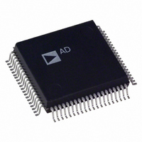
AD1843JS Analog Devices Inc, AD1843JS Datasheet - Page 49

AD1843JS
Manufacturer Part Number
AD1843JS
Description
IC CODEC STEREO 5V 16BIT 80PQFP
Manufacturer
Analog Devices Inc
Type
Stereo Audior
Datasheet
1.AD1843JS.pdf
(64 pages)
Specifications of AD1843JS
Rohs Status
RoHS non-compliant
Data Interface
Serial
Resolution (bits)
16 b
Number Of Adcs / Dacs
1 / 2
Sigma Delta
Yes
S/n Ratio, Adcs / Dacs (db) Typ
92 / 86
Dynamic Range, Adcs / Dacs (db) Typ
85 / 80
Voltage - Supply, Analog
4.75 V ~ 5.25 V
Voltage - Supply, Digital
2.85 V ~ 5.25 V
Operating Temperature
0°C ~ 70°C
Mounting Type
Surface Mount
Package / Case
80-MQFP, 80-PQFP
Available stocks
Company
Part Number
Manufacturer
Quantity
Price
Part Number:
AD1843JS
Manufacturer:
ADI/亚德诺
Quantity:
20 000
REV. 0
ADREN
ADLEN
res
PDNI
ACEN
C3EN
Address 28
Data 15
ENCV3
Data 7
PDNI
ADC Right Channel Enable/Power Down. When this bit is reset to “0,” the right ADC channel is powered down and
serial interface sample output will cease after the current frame. When this bit is set to “1,” the right ADC channel is
enabled and sampling of analog input will begin on the first rising edge of the conversion clock (CONV pin) after the
sixth rising edge of frame sync (SDFS pin). This delay allows the ADC startup to be similar to the DAC startup, and
allows some time for stale ADC data inside the AD1843 to be cleared. It also allows the serial interface to synchronize
with the conversion clock, which is potentially already running. Multiple ADCs on multiple AD1843s which share the
same frame sync will be synchronously started if they are enabled at any time during the same frame.
0 = ADC Right Channel is Powered Down
1 = ADC Right Channel is Enabled
ADC Left Channel Enable/Power Down. When this bit is reset to “0,” the left ADC channel is powered down and
serial interface sample output will cease after the current frame. When this bit is set to “1,” the left ADC channel is
enabled and sampling of analog input will begin on the first rising edge of the conversion clock (CONV pin) after the
sixth rising edge of frame sync (SDFS pin). This delay allows the ADC startup to be similar to the DAC startup, and
allows some time for stale ADC data inside the AD1843 to be cleared. It also allows the serial interface to synchronize
with the conversion clock, which is potentially already running. Multiple ADCs on multiple AD1843s which share the
same frame sync will be synchronously started if they are enabled at any time during the same frame.
0 = ADC Left Channel is Powered Down
1 = ADC Left Channel is Enabled
Reserved for future expansion. To ensure future compatibility, write “0” to all reserved bits.
Initial default state after reset: 0000 0000 1100 0000 (00C0 hex). Cleared to default and cannot be written to when:
the RESET pin is asserted LO; when the PWRDWN pin is asserted LO; or when the PDNO bit in Control Register
Address 0 is set to “1” (all conversions disabled).
Converter Power Down. When set to “1,” this bit initiates the process of powering down all conversion channels,
overriding the settings in Control Register Address 27. Unlike the individual power down bits in Control Register
Address 27, asserting this bit allows the DAC and V
results in lower power consumption than results from powering down all channels individually through Control Regis-
ter Address 27, and also reduces speaker “click” if asserted before the power supply is removed. Power down is not
complete until approximately 5 ms after this bit is set to “1.” During this time, the AD1843 still requires a clock in-
put from XTALI for proper operation. When reset to “0,” this bit initiates the process of preparing the AD1843 for
conversions after power down. Approximately 470 ms are necessary to exit power down. The power up/down status
of the AD1843 may be monitored through the PDNO bit in Control Register Address 0. Asserting the power down
pin (PWRDWN) will result in an even greater degree of power down as it also powers down the serial interface and
crystal oscillator. Once a power up or power down sequence has been initiated, its completion cannot be interrupted.
Changes made to the state of PDNI (i.e., writes to PDNI) are ignored until a previously pending PDNI state change
has been completely processed.
0 = Normal (Non-Power Down) Operation
1 = Initiate Power Down of All Conversion Channels
Autocalibration Enable. When set to “1,” autocalibration will occur each time power down is exited (PDNI is
changed from a “1” to a “0”). Autocalibration increases the time required to exit power down by 4 ms (from
470 ms to 474 ms). When reset to “0,” autocalibration is disabled. This bit is set to “1” initially after reset and can-
not be overwritten until after the AD1843 has come out of power down (PDNO bit in Control Register Address 0
reset to “0”) at least once. Note that an autocalibration cycle is always performed following a hardware reset (i.e.,
RESET pin asserted) or a hardware power down (i.e., PWRDWN pin asserted), regardless of the state of ACEN.
0 = Autocalibration Disabled
1 = Autocalibration Enabled, Initiated upon Exiting Power Down
Clock Generator 3 Enable/Power Down.
0 = Clock Generator 3 Powered Down
1 = Clock Generator 3 Enabled
Data 14
ENBT3
ACEN
Data 6
Codec Configuration—Fundamental Settings
Data 13
ENCV2
Data 5
C3EN
Data 12
ENBT2
Data 4
C2EN
–49–
REF
Data 11
ENCV1
Data 3
C1EN
output pins to slowly decay to ground. Setting this bit to “1”
ENCLKO
Data 10
ENBT1
Data 2
LINRSD
XCTL1
Data 9
Data 1
LINLSD
XCTL0
Data 8
Data 0
AD1843


