AD1843JS Analog Devices Inc, AD1843JS Datasheet - Page 48
AD1843JS
Manufacturer Part Number
AD1843JS
Description
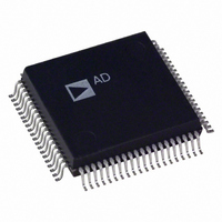
IC CODEC STEREO 5V 16BIT 80PQFP
Manufacturer
Analog Devices Inc
Type
Stereo Audior
Datasheet
1.AD1843JS.pdf
(64 pages)
Specifications of AD1843JS
Rohs Status
RoHS non-compliant
Data Interface
Serial
Resolution (bits)
16 b
Number Of Adcs / Dacs
1 / 2
Sigma Delta
Yes
S/n Ratio, Adcs / Dacs (db) Typ
92 / 86
Dynamic Range, Adcs / Dacs (db) Typ
85 / 80
Voltage - Supply, Analog
4.75 V ~ 5.25 V
Voltage - Supply, Digital
2.85 V ~ 5.25 V
Operating Temperature
0°C ~ 70°C
Mounting Type
Surface Mount
Package / Case
80-MQFP, 80-PQFP
Available stocks
Company
Part Number
Manufacturer
Quantity
Price

Part Number:
AD1843JS
Manufacturer:
ADI/亚德诺
Quantity:
20 000


AD1843
DFREE
DDMEN
DA2EN
DA1EN
ANAEN
HPEN
AAMEN
Address 27
Data 15
ANAEN
DFREE
Data 7
Digital Resource Free. When set to “1,” this bit reduces the level of power down normally achieved by asserting the
DAC2 to DAC1 Mix Enable/Power Down. When reset to “0,” Control Register Address 3 is cleared to its default
DAC2 (Left and Right Channels) Enable/Power Down. When this bit is reset to “0,” DAC2 is powered down and
DAC1 (Left and Right Channels) Enable/Power Down. When this bit is reset to “0,” DAC1 is powered down and
Analog Channel Enable/Power Down. If this bit is reset to “0,” all analog conversion circuitry (related to bits
Headphone Enable/Power Down.
Analog Input to Analog Output Mix Enable/Power Down. When reset to “0,” Control Register Addresses 4 - 7 and
power down bits in this Control Register. However, it allows the digital resources of channels powered down to be
partially transferred to the remaining enabled channels and thus permits conversion rates higher than the 48 kHz
nominal maximum. See the “Supported Conversion Rates” section.
0 = Power Down of Digital Resources is Complete
1 = Power Down of Digital Resources is Incomplete, Freeing Transferable Resources to Enabled Channels
and cannot be written.
0 = Mix is Powered Down
1 = Mix is Enabled
serial interface requests for samples (see slot 0) will cease immediately. When this bit is set to “1,” DAC2 is enabled
and requests for samples resume on the next frame. Conversions will not actually begin until the first rising edge of
the conversion clock (CONV pin) after the sixth rising edge of frame sync (SDFS pin) after this bit is set to “1.” This
delay allows the four word stereo input buffer for DAC2 to be filled before conversions begin and allows the serial in-
terface to synchronize with the conversion clock, which is potentially already running. This delay also allows DACs
on multiple AD1843s sharing the same frame sync to begin conversions synchronously, providing they are enabled at
any time during the same frame. When this bit is reset to “0,” Control Register Address 10, which is the Output
Level Control Register for DAC2, is cleared to default and cannot be written.
0 = DAC2 is Powered Down, Control Register Address 10 (DAC2 Output Level Control) is Cleared
1 = DAC2 is Enabled
serial interface requests for samples (see slot 0) will cease immediately. When this bit is set to “1,” DAC1 is enabled
and requests for samples resume on the next frame. Conversions will not actually begin until the first rising edge of
the conversion clock (CONV pin) after the sixth rising edge of frame sync (SDFS pin) after this bit is set to “1.” This
delay allows the four word stereo input buffer for DAC1 to be filled before conversions begin and allows the serial in-
terface to synchronize with the conversion clock, which is potentially already running. This delay also allows DACs
on multiple AD1843s sharing the same frame sync to begin conversions synchronously, providing they are enabled at
any time during the same frame. When this bit is reset to “0,” Control Register Address 9, which is the Output Level
Control Register for DAC1, is cleared to default and cannot be written.
0 = DAC1 is Powered Down, Control Register Address 9 (DAC1 Output Level Control) is Cleared
1 = DAC1 is Enabled
DA1EN, DA2EN, ADLEN, ADREN, DDMEN and AAMEN) will be powered down. When reset to “0,” the only
conversion channels usable (but must be enabled separately) are the digital resampling paths. Since resetting this bit
to “0” powers down the analog ADC, DAC1, DAC2 and analog mixers, their related output level Control Register
Addresses 4 through 7, half of 8, 9 and 10 are cleared and cannot be written while ANAEN remains “0.”
0 = Analog Channels are Powered Down, Control Register Addresses 4 through 7, half of 8, 9 and 10 are Cleared to
1 = Analog DAC and ADC Paths are Controlled by DA1EN, DA2EN, ADLEN, ADREN, DDMEN and AAMEN
0 = Headphone Output is Powered Down
1 = Headphone Output is Enabled
half of Control Register Address 8 are cleared and cannot be written.
0 = Mix is Powered Down
1 = Mix is Enabled
Default (Digital to Digital Still Possible)
Data 14
Data 6
HPEN
res
Codec Configuration—Channel Power Down
Data 13
Data 5
res
res
DDMEN
AAMEN
Data 12
Data 4
–48–
Data 11
Data 3
res
res
Data 10
Data 2
res
res
ADREN
DA2EN
Data 9
Data 1
DA1EN
ADLEN
Data 8
Data 0
REV. 0
Related parts for AD1843JS
Image
Part Number
Description
Manufacturer
Datasheet
Request
R

Part Number:
Description:
±1.7g Dual-Axis IMEMS Accelerometer Evaluation Board
Manufacturer:
Analog Devices Inc
Datasheet:

Part Number:
Description:
Inertial Sensor Evaluation System
Manufacturer:
Analog Devices Inc
Datasheet:
Part Number:
Description:
Manufacturer:
Analog Devices Inc
Datasheet:
Part Number:
Description:
Manufacturer:
Analog Devices Inc
Datasheet:
Part Number:
Description:
Manufacturer:
Analog Devices Inc
Datasheet:
Part Number:
Description:
Manufacturer:
Analog Devices Inc
Datasheet:
Part Number:
Description:
Manufacturer:
Analog Devices Inc
Datasheet:
Part Number:
Description:
Manufacturer:
Analog Devices Inc
Datasheet:
Part Number:
Description:
Manufacturer:
Analog Devices Inc
Datasheet:
Part Number:
Description:
Manufacturer:
Analog Devices Inc
Datasheet:
Part Number:
Description:
Manufacturer:
Analog Devices Inc
Datasheet:
Part Number:
Description:
Manufacturer:
Analog Devices Inc
Datasheet:
Part Number:
Description:
Manufacturer:
Analog Devices Inc
Datasheet: