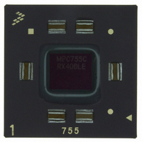
MPC755CRX400LE Freescale Semiconductor, MPC755CRX400LE Datasheet - Page 41

MPC755CRX400LE
Manufacturer Part Number
MPC755CRX400LE
Description
IC MPU 32BIT 400MHZ PPC 360-CBGA
Manufacturer
Freescale Semiconductor
Datasheet
1.MPC755BPX300LE.pdf
(56 pages)
Specifications of MPC755CRX400LE
Processor Type
MPC7xx PowerPC 32-Bit
Speed
400MHz
Voltage
2V
Mounting Type
Surface Mount
Package / Case
360-FCCBGA
Family Name
MPC7xx
Device Core
PowerPC
Device Core Size
64b
Frequency (max)
400MHz
Instruction Set Architecture
RISC
Supply Voltage 1 (typ)
2V
Operating Supply Voltage (max)
2.1V
Operating Supply Voltage (min)
1.9V
Operating Temp Range
0C to 105C
Operating Temperature Classification
Commercial
Mounting
Surface Mount
Pin Count
360
Package Type
FCCBGA
Lead Free Status / RoHS Status
Contains lead / RoHS non-compliant
Features
-
Lead Free Status / Rohs Status
Not Compliant
Available stocks
Company
Part Number
Manufacturer
Quantity
Price
Company:
Part Number:
MPC755CRX400LE
Manufacturer:
MOT
Quantity:
12 388
Company:
Part Number:
MPC755CRX400LE
Manufacturer:
Freescale Semiconductor
Quantity:
10 000
Table 18
65°, and 105°C. The impedance increases with junction temperature and is relatively unaffected by bus
voltage.
8.6
The MPC755 requires pull-up resistors (1−5 kΩ) on several control pins of the bus interface to maintain
the control signals in the negated state after they have been actively negated and released by the MPC755
or other bus masters. These pins are TS, ABB, AACK, ARTRY, DBB, DBWO, TA, TEA, and DBDIS.
DRTRY should also be connected to a pull-up resistor (1−5 kΩ) if it will be used by the system; otherwise,
this signal should be connected to HRESET to select NO-DRTRY mode (see the MPC750 RISC
Microprocessor Family User’s Manual for more information on this mode).
Three test pins also require pull-up resistors (100 Ω−1 kΩ). These pins are L1_TSTCLK, L2_TSTCLK,
and LSSD_MODE. These signals are for factory use only and must be pulled up to OV
machine operation.
In addition, CKSTP_OUT is an open-drain style output that requires a pull-up resistor (1−5 kΩ) if it is used
by the system.
During inactive periods on the bus, the address and transfer attributes may not be driven by any master and
may, therefore, float in the high-impedance state for relatively long periods of time. Since the MPC755
must continually monitor these signals for snooping, this float condition may cause additional power draw
by the input receivers on the MPC755 or by other receivers in the system. These signals can be pulled up
through weak (10-kΩ) pull-up resistors by the system or may be otherwise driven by the system during
inactive periods of the bus to avoid this additional power draw, but address bus pull-up resistors are not
necessary for proper device operation. The snooped address and transfer attribute inputs are: A[0:31],
AP[0:3], TT[0:4], TBST, and GBL.
The data bus input receivers are normally turned off when no read operation is in progress and, therefore,
do not require pull-up resistors on the bus. Other data bus receivers in the system, however, may require
pull-ups, or that those signals be otherwise driven by the system during inactive periods by the system. The
data bus signals are: DH[0:31], DL[0:31], and DP[0:7].
If 32-bit data bus mode is selected, the input receivers of the unused data and parity bits will be disabled,
and their outputs will drive logic zeros when they would otherwise normally be driven. For this mode,
these pins do not require pull-up resistors, and should be left unconnected by the system to minimize
possible output switching.
If address or data parity is not used by the system, and the respective parity checking is disabled through
HID0, the input receivers for those pins are disabled, and those pins do not require pull-up resistors and
Freescale Semiconductor
summarizes the signal impedance results. The driver impedance values were characterized at 0°,
Pull-Up Resistor Requirements
MPC755 RISC Microprocessor Hardware Specifications, Rev. 8
Impedance
R
R
N
P
Table 18. Impedance Characteristics
V
Processor Bus
DD
= 2.0 V, OV
25–36
26
–
39
DD
= 3.3 V, T
L2 Bus
25–36
26–39
j
= 0°–105°C
Symbol
Z
Z
0
0
Unit
Ω
Ω
System Design Information
DD
for normal
41


