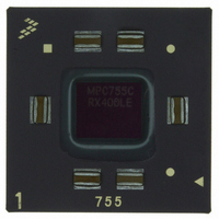
MPC755CRX400LE Freescale Semiconductor, MPC755CRX400LE Datasheet - Page 20

MPC755CRX400LE
Manufacturer Part Number
MPC755CRX400LE
Description
IC MPU 32BIT 400MHZ PPC 360-CBGA
Manufacturer
Freescale Semiconductor
Datasheet
1.MPC755BPX300LE.pdf
(56 pages)
Specifications of MPC755CRX400LE
Processor Type
MPC7xx PowerPC 32-Bit
Speed
400MHz
Voltage
2V
Mounting Type
Surface Mount
Package / Case
360-FCCBGA
Family Name
MPC7xx
Device Core
PowerPC
Device Core Size
64b
Frequency (max)
400MHz
Instruction Set Architecture
RISC
Supply Voltage 1 (typ)
2V
Operating Supply Voltage (max)
2.1V
Operating Supply Voltage (min)
1.9V
Operating Temp Range
0C to 105C
Operating Temperature Classification
Commercial
Mounting
Surface Mount
Pin Count
360
Package Type
FCCBGA
Lead Free Status / RoHS Status
Contains lead / RoHS non-compliant
Features
-
Lead Free Status / Rohs Status
Not Compliant
Available stocks
Company
Part Number
Manufacturer
Quantity
Price
Company:
Part Number:
MPC755CRX400LE
Manufacturer:
MOT
Quantity:
12 388
Company:
Part Number:
MPC755CRX400LE
Manufacturer:
Freescale Semiconductor
Quantity:
10 000
Electrical and Thermal Characteristics
Figure 8
20
L2SYNC_IN to high impedance:
Notes:
1. Rise and fall times for the L2SYNC_IN input are measured from 20% to 80% of L2OV
2. All input specifications are measured from the midpoint of the signal in question to the midpoint voltage of the rising edge of
3. All output specifications are measured from the midpoint voltage of the rising edge of L2SYNC_IN to the midpoint of the
4. The outputs are valid for both single-ended and differential L2CLK modes. For pipelined registered synchronous BurstRAMs,
5. Guaranteed by design and characterization.
6. Revisions prior to Rev. 2.8 (Rev. E) were limited in performance and did not conform to this specification. For more
At recommended operating conditions (see
the input L2SYNC_IN (see
signal in question. The output timings are measured at the pins. All output timings assume a purely resistive 50-Ω load (see
Figure
L2CR[14–15] = 01 or 10 is recommended. For pipelined late write synchronous BurstRAMs, L2CR[14–15] = 11 is
recommended.
information, refer to
L2 Data and Data
10).
shows the L2 bus input timing diagrams for the MPC755.
Parity Inputs
L2SYNC_IN
Section 10.2, “Part Numbers Not Fully Addressed by This Document.”
Parameter
All outputs when L2CR[14–15] = 00
All outputs when L2CR[14–15] = 01
All outputs when L2CR[14–15] = 10
All outputs when L2CR[14–15] = 11
Table 12. L2 Bus Interface AC Timing Specifications (continued)
MPC755 RISC Microprocessor Hardware Specifications, Rev. 8
Figure
8). Input timings are measured at the pins.
Figure 8. L2 Bus Input Timing Diagrams
Table
3)
VM = Midpoint Voltage (L2OV
t
DVL2CH
Symbol
t
L2CHOZ
VM
DD
t
DXL2CH
/2)
All Speed Grades
Min
—
—
—
—
t
L2CR
DD
.
Max
2.4
2.6
2.8
3.0
Freescale Semiconductor
Unit
ns
t
L2CF
Notes
3, 5


