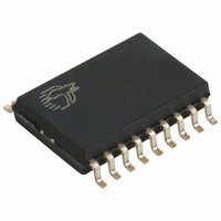
CY7C63723C-SXC Cypress Semiconductor Corp, CY7C63723C-SXC Datasheet - Page 3

CY7C63723C-SXC
Manufacturer Part Number
CY7C63723C-SXC
Description
IC MCU 8K LS USB/PS-2 18-SOIC
Manufacturer
Cypress Semiconductor Corp
Series
enCoRe™r
Datasheet
1.CY7C63723C-SXC.pdf
(53 pages)
Specifications of CY7C63723C-SXC
Package / Case
18-SOIC (7.5mm Width)
Applications
USB Microcontroller
Core Processor
M8B
Program Memory Type
OTP (8 kB)
Controller Series
CY7C637xx
Ram Size
256 x 8
Interface
PS2, USB
Number Of I /o
10
Voltage - Supply
3.5 V ~ 5.5 V
Operating Temperature
0°C ~ 70°C
Mounting Type
Surface Mount
Product
USB and PS/2 Controller
Number Of I/os
10
Operating Supply Voltage
11 V
Supply Current (max)
20 mA
Maximum Operating Temperature
+ 70 C
Minimum Operating Temperature
0 C
Mounting Style
SMD/SMT
Maximum Power Dissipation
300 mW
Number Of Timers
4
Core Size
8 Bit
No. Of I/o's
10
Program Memory Size
8KB
Ram Memory Size
256Byte
Cpu Speed
12MHz
No. Of Timers
1
Embedded Interface Type
PS/2, USB
Digital Ic Case Style
SOIC
Rohs Compliant
Yes
Lead Free Status / RoHS Status
Lead free / RoHS Compliant
Lead Free Status / RoHS Status
Lead free / RoHS Compliant, Lead free / RoHS Compliant
Other names
428-1855
Available stocks
Company
Part Number
Manufacturer
Quantity
Price
Company:
Part Number:
CY7C63723C-SXC
Manufacturer:
CYPRESS
Quantity:
12 000
Part Number:
CY7C63723C-SXC
Manufacturer:
CYPRESS/赛普拉斯
Quantity:
20 000
event, and subtracting the two values. The four capture timers
save a programmable 8 bit range of the free-running timer when
a GPIO edge occurs on the two capture pins (P0.0, P0.1).
The CY7C637xxC includes an integrated USB serial interface
engine (SIE) that supports the integrated peripherals. The
hardware supports one USB device address with three
endpoints. The SIE allows the USB host to communicate with the
function integrated into the microcontroller. A 3.3V regulated
output pin provides a pull-up source for the external USB resistor
on the D– pin.
Pin Configurations
Pin Definitions
Document #: 38-08022 Rev. *D
D–/SDATA,
D+/SCLK
P0[7:0]
P1[7:0]
XTALIN/P2.1
XTALOUT
V
V
VREG/P2.0
V
PP
CC
SS
Name
XTALIN/P2.1
VREG/P2.0
18-pin SOIC/PDIP
P0.0
P0.1
P0.2
P0.3
P1.0
VSS
VPP
CY7C63723C
OUT
I/O
I/O
I/O
I/O
1
2
3
4
5
6
7
8
9
IN
18
17
16
15
14
13
12
11
10
CY7C63723C CY7C63743C CY7C63722C
15, 16, 17, 18
1, 2, 3, 4,
18-Pin
P0.5
P0.4
P0.6
P0.7
P1.1
D+/SCLK
D–/SDATA
VCC
XTALOUT
5, 14
12
13
10
11
9
7
8
6
21, 22, 23, 24
17, 18, 19, 20
1, 2, 3, 4,
5, 6, 7, 8,
24-Pin
15
16
12
13
10
14
11
XTALIN/P2.1
9
VREG/P2.0
24-pin SOIC/PDIP/QSOP
P0.0
P0.1
P0.2
P0.3
P1.0
P1.2
P1.4
P1.6
VSS
VPP
CY7C63743C
22, 23, 24, 25
18, 19, 20, 21
1
2
3
4
5
6
7
8
9
10
11
12
1, 2, 3, 4,
5, 6, 7, 8,
Top View
25-Pad
9, 10
16
17
13
14
11
15
12
24
23
22
21
20
19
18
17
16
15
14
13
P0.4
P0.5
P0.6
P0.7
P1.1
P1.3
P1.5
P1.7
D+/SCLK
D–/SDATA
VCC
XTALOUT
The USB D+ and D– USB pins can alternately be used as PS/2
SCLK and SDATA signals, so that products can be designed to
respond to either USB or PS/2 modes of operation. PS/2
operation is supported with internal pull-up resistors on SCLK
and SDATA, the ability to disable the regulator output pin, and an
interrupt to signal the start of PS/2 activity. No external compo-
nents are necessary for dual USB and PS/2 systems, and no
GPIO pins need to be dedicated to switching between modes.
Slow edge rates operate in both modes to reduce EMI.
USB differential data lines (D– and D+), or PS/2 clock
and data signals (SDATA and SCLK)
GPIO Port 0 capable of sinking up to 50 mA/pin, or
sinking controlled low or high programmable current.
Can also source 2 mA current, provide a resistive
pull-up, or serve as a high-impedance input. P0.0 and
P0.1 provide inputs to Capture Timers A and B, respec-
tively.
IO Port 1 capable of sinking up to 50 mA/pin, or sinking
controlled low or high programmable current. Can also
source 2 mA current, provide a resistive pull-up, or
serve as a high-impedance input.
6-MHz ceramic resonator or external clock input, or
P2.1 input
6-MHz ceramic resonator return pin or internal oscillator
output
Programming voltage supply, ground for normal
operation
Voltage supply
Voltage supply for 1.3-kΩ USB pull-up resistor (3.3V
nominal). Also serves as P2.0 input.
Ground
P0.3
P1.0
P1.2
P1.4
P1.6
VSS
VSS
CY7C63722C-XC
Description
10
4
5
6
7
8
9
DIE
17
22
21
20
19
18
P0.7
P1.1
P1.3
P1.5
P1.7
D+/SCLK
CY7C63722C
CY7C63723C
CY7C63743C
Page 3 of 53
[+] Feedback


