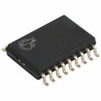
CY7C63723C-SXC Cypress Semiconductor Corp, CY7C63723C-SXC Datasheet - Page 24

CY7C63723C-SXC
Manufacturer Part Number
CY7C63723C-SXC
Description
IC MCU 8K LS USB/PS-2 18-SOIC
Manufacturer
Cypress Semiconductor Corp
Series
enCoRe™r
Datasheet
1.CY7C63723C-SXC.pdf
(53 pages)
Specifications of CY7C63723C-SXC
Package / Case
18-SOIC (7.5mm Width)
Applications
USB Microcontroller
Core Processor
M8B
Program Memory Type
OTP (8 kB)
Controller Series
CY7C637xx
Ram Size
256 x 8
Interface
PS2, USB
Number Of I /o
10
Voltage - Supply
3.5 V ~ 5.5 V
Operating Temperature
0°C ~ 70°C
Mounting Type
Surface Mount
Product
USB and PS/2 Controller
Number Of I/os
10
Operating Supply Voltage
11 V
Supply Current (max)
20 mA
Maximum Operating Temperature
+ 70 C
Minimum Operating Temperature
0 C
Mounting Style
SMD/SMT
Maximum Power Dissipation
300 mW
Number Of Timers
4
Core Size
8 Bit
No. Of I/o's
10
Program Memory Size
8KB
Ram Memory Size
256Byte
Cpu Speed
12MHz
No. Of Timers
1
Embedded Interface Type
PS/2, USB
Digital Ic Case Style
SOIC
Rohs Compliant
Yes
Lead Free Status / RoHS Status
Lead free / RoHS Compliant
Lead Free Status / RoHS Status
Lead free / RoHS Compliant, Lead free / RoHS Compliant
Other names
428-1855
Available stocks
Company
Part Number
Manufacturer
Quantity
Price
Company:
Part Number:
CY7C63723C-SXC
Manufacturer:
CYPRESS
Quantity:
12 000
Part Number:
CY7C63723C-SXC
Manufacturer:
CYPRESS/赛普拉斯
Quantity:
20 000
SPI Interrupt
For SPI, an interrupt request is generated after a byte is received
or transmitted. See Section for details on the SPI interrupt.
SPI Modes for GPIO Pins
The GPIO pins used for SPI outputs (P0.5–P0.7) contain a
bypass mode, as shown in the GPIO block diagram (Figure ).
Whenever the SPI block is inactive (Mode[5:4] = 00), the bypass
value is 1, which enables normal GPIO operation. When SPI
Table 5. SPI Pin Assignments
Document #: 38-08022 Rev. *D
Master Out, Slave In (MOSI)
Master In, Slave Out (MISO)
Slave Select (SS)
CPHA = 0:
CPHA = 1:
SCK (CPOL = 0)
SCK (CPOL = 1)
SS
MOSI/MISO
Data Capture Strobe
Interrupt Issued
MOSI/MISO
Data Capture Strobe
Interrupt Issued
SPI Function
SCK
x
MSB
MSB
GPIO Pin
P0.4
P0.6
P0.7
P0.5
Figure 23. SPI Data Timing
For master mode, firmware sets SS, may use any GPIO pin.
For Slave Mode, SS is an active LOW input.
Data output for master, data input for slave.
Data input for master, data output for slave.
SPI Clock: Output for master, input for slave.
master or slave modes are activated, the appropriate bypass
signals are driven by the hardware for outputs, and are held at 1
for inputs. Note that the corresponding data bits in the Port 0
Data Register must be set to 1 for each pin being used for
an SPI output. In addition, the GPIO modes are not affected by
operation of the SPI block, so each pin must be programmed by
firmware to the desired drive strength mode.
For GPIO pins that are not used for SPI outputs, the SPI bypass
value in Figure is always 1, for normal GPIO operation.
Comment
LSB
LSB
CY7C63722C
CY7C63723C
CY7C63743C
x
Page 24 of 53
[+] Feedback


