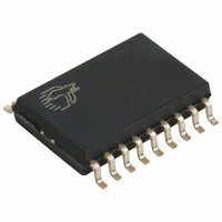
CY7C63723C-SXC Cypress Semiconductor Corp, CY7C63723C-SXC Datasheet - Page 18

CY7C63723C-SXC
Manufacturer Part Number
CY7C63723C-SXC
Description
IC MCU 8K LS USB/PS-2 18-SOIC
Manufacturer
Cypress Semiconductor Corp
Series
enCoRe™r
Datasheet
1.CY7C63723C-SXC.pdf
(53 pages)
Specifications of CY7C63723C-SXC
Package / Case
18-SOIC (7.5mm Width)
Applications
USB Microcontroller
Core Processor
M8B
Program Memory Type
OTP (8 kB)
Controller Series
CY7C637xx
Ram Size
256 x 8
Interface
PS2, USB
Number Of I /o
10
Voltage - Supply
3.5 V ~ 5.5 V
Operating Temperature
0°C ~ 70°C
Mounting Type
Surface Mount
Product
USB and PS/2 Controller
Number Of I/os
10
Operating Supply Voltage
11 V
Supply Current (max)
20 mA
Maximum Operating Temperature
+ 70 C
Minimum Operating Temperature
0 C
Mounting Style
SMD/SMT
Maximum Power Dissipation
300 mW
Number Of Timers
4
Core Size
8 Bit
No. Of I/o's
10
Program Memory Size
8KB
Ram Memory Size
256Byte
Cpu Speed
12MHz
No. Of Timers
1
Embedded Interface Type
PS/2, USB
Digital Ic Case Style
SOIC
Rohs Compliant
Yes
Lead Free Status / RoHS Status
Lead free / RoHS Compliant
Lead Free Status / RoHS Status
Lead free / RoHS Compliant, Lead free / RoHS Compliant
Other names
428-1855
Available stocks
Company
Part Number
Manufacturer
Quantity
Price
Company:
Part Number:
CY7C63723C-SXC
Manufacturer:
CYPRESS
Quantity:
12 000
Part Number:
CY7C63723C-SXC
Manufacturer:
CYPRESS/赛普拉斯
Quantity:
20 000
Table 4. Control Modes to Force D+/D– Outputs
USB Device
The CY7C637xxC supports one USB Device Address with three
endpoints: EP0, EP1, and EP2.
USB Address Register
The USB Device Address Register contains a 7-bit USB address
and one bit to enable USB communication. This register is
cleared during a reset, setting the USB device address to zero
and marking this address as disabled.
format of the USB Address Register.
Figure 15. USB Device Address Register (Address 0x10)
In either USB or PS/2 mode, this register is cleared by both hard-
ware resets and the USB bus reset. See Section for more infor-
mation on the USB Bus Reset – PS/2 interrupt.
Bit 7: Device Address Enable
Bit [6:0]: Device Address Bit [6:0]
Document #: 38-08022 Rev. *D
Note
Read/Write
2. For PS/2 operation, the D+/D– Forcing Bit [2:0] = 111b mode must be set initially (one time only) before using the other PS/2 force modes
Forcing Bit
Bit Name
This bit must be enabled by firmware before the serial inter-
face engine (SIE) will respond to USB traffic at the address
specified in Bit [6:0].
1 = Enable USB device address.
0 = Disable USB device address.
These bits must be set by firmware during the USB enumer-
ation process (i.e., SetAddress) to the non-zero address as-
signed by the USB host.
Reset
Bit #
D+/D–
[2:0]
000
001
010
100
101
011
110
111
Address
Device
Enable
Not forcing (SIE controls
driver)
Force K (D+ HIGH, D– LOW)
Force J (D+ LOW, D– HIGH)
Force SE0 (D– LOW, D+
LOW)
Force D– LOW, D+ LOW
Force D– LOW, D+ HiZ
Force D– HiZ, D+ LOW
Force D– HiZ, D+ HiZ
R/W
7
0
Control Action
R/W R/W R/W R/W R/W R/W R/W
6
0
5
0
Device Address
4
0
Figure 15
3
0
2
0
USB Mode
shows the
Any Mode
Mode
cation
Appli-
PS/2
1
0
[2]
0
0
USB Control Endpoint
All USB devices are required to have an endpoint number 0
(EP0) that is used to initialize and control the USB device. EP0
provides access to the device configuration information and
allows generic USB status and control accesses. EP0 is bidirec-
tional as the device can both receive and transmit data. EP0
uses an 8-byte FIFO at SRAM locations 0xF8-0xFF, as shown in
Section .
The EP0 endpoint mode register uses the format shown in
Figure
Figure 16. Endpoint 0 Mode Register (Address 0x12)
The SIE provides a locking feature to prevent firmware from
overwriting bits in the USB Endpoint 0 Mode Register. Writes to
the register have no effect from the point that Bit[6:0] of the
register are updated (by the SIE) until the firmware reads this
register. The CPU can unlock this register by reading it.
Because of these hardware-locking features, firmware should
perform an read after a write to the USB Endpoint 0 Mode
Register and USB Endpoint 0 Count Register
verify that the contents have changed as desired, and that the
SIE has not updated these values.
Bit [7:4] of this register are cleared by any non-locked write to
this register, regardless of the value written.
Bit 7: SETUP Received
Bit 6: IN Received
Name
Read/
Reset
Write
Bit #
Bit
1 = A valid SETUP packet has been received. This bit is
forced HIGH from the start of the data packet phase of the
SETUP transaction until the start of the ACK packet returned
by the SIE. The CPU is prevented from clearing this bit during
this interval. While this bit is set to ‘1’, the CPU cannot write
to the EP0 FIFO. This prevents firmware from overwriting an
incoming SETUP transaction before firmware has a chance
to read the SETUP data.
0 = No SETUP received. This bit is cleared by any non-locked
writes to the register.
1 = A valid IN packet has been received. This bit is updated
to ‘1’ after the last received packet in an IN transaction. This
bit is cleared by any non-locked writes to the register.
0 = No IN received. This bit is cleared by any non-locked
writes to the register.
16.
Received
SETUP
R/W
7
0
Received
R/W
IN
6
0
Received
OUT
R/W
5
0
Transaction
ACKed
CY7C63722C
CY7C63723C
CY7C63743C
R/W
4
0
(Figure
Page 18 of 53
0 0 0 0
Mode Bit
18) to
R/W
3:0
[+] Feedback


