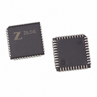
Z8927320VSG Zilog, Z8927320VSG Datasheet - Page 41

Z8927320VSG
Manufacturer Part Number
Z8927320VSG
Description
DSP 20MHZ 16-BIT W/ A/D 44-PLCC
Manufacturer
Zilog
Series
Z892x3r
Type
Fixed Pointr
Datasheet
1.Z8937320FSC00TR.pdf
(60 pages)
Specifications of Z8927320VSG
Interface
SPI, 3-Wire Serial
Clock Rate
20MHz
Non-volatile Memory
OTP (16 kB)
On-chip Ram
1kB
Voltage - I/o
5.00V
Voltage - Core
5.00V
Operating Temperature
0°C ~ 70°C
Mounting Type
Surface Mount
Package / Case
44-LCC (J-Lead)
Lead Free Status / RoHS Status
Lead free / RoHS Compliant
Available stocks
Company
Part Number
Manufacturer
Quantity
Price
Company:
Part Number:
Z8927320VSG
Manufacturer:
Zilog
Quantity:
50
ZiLOG
C/T Registers
Each C/T contains a set of five 16-bit Registers. Bank13 is
used to access the registers for C/T0 and Bank14 is for the
C/T1 registers. All accesses to C/T Registers occur with
zero wait states.
Counter/Timer Control Register (Bank13,14/EXT1).
C/T Control register enables/disables the C/T, selects input
and output options, and the mode of operation.
TMLR—Load Register (Bank13,14/EXT2).
TMLR register holds the value that is loaded into TMR
when TMR underflows.
TMR—Counter Register (Bank13,14/EXT3).
16-bit down counter that holds the current C/T value. It can
be read like any other ordinary register. However, writing
DS000202-DSP0599
Bank 13/EXT1 (C/T0) and Bank14/EXT1 (C/T1)
D15 D14 D13 D12 D11 D10 D9 D8
*Note: The user should always program this bit to "0".
Figure 32. C/T0 and C/T1 Control Register
D7
D6
T h e 1 6 - b i t
TMR is a
D5
D4 D3
The
D2
D1 D0
to TMR is different than writing to an ordinary register. A
write to TMR causes the contents of TMLR to be written
into TMR, causing the C/T to be retriggered.
TPLR—Prescaler Load Register (Bank13,14/EXT4).
16-bit TPLR register holds the prescaler load value in its
lower 8 bits. Bit 15 must be written with a “1”, and bits 14–8
must be written with “0’s”.
Note: If the C/T interrupt is being used, this register must be re-
16-Bit Digital Signal Processors with A/D Converter
written at the end of the interrupt service routine in order
to enable the next interrupt. The number of clock cycles
from the beginning of the interrupt service routine to the
write must exceed the prescaler load value.
C/T
Input Select
Input Event
Output Select
Output Polarity
Mode of Operation
Reserved
Test Mode*
0 = Disabled (default)
1 = Enabled
00 = Inputs have no effect (default)
01 = Reserved
10 = UI0 Pin
11 = UI1 Pin
00 = Falling Edge (default)
01 = Rising Edge
10 = Both Rising and Falling Edges
11 = Reserved
00 = Outputs Unaffected (default)
01 = Reserved
10 = Drive TMO0 Pin
11 = Reserved
0 = Output asserted High on Timeout (default)
1 = Output asserted Low on Timeout
0000 = Square Wave Output (default)
0001 = Retriggerable One-Shot
0010 = PWM (8-bit)
0011 = PWM (16-bit)
0100 = Finite Pulse String Generator
0101 = Externally-Clocked One-Shot
0110 = Software Watch-Dog Timer
0111 = Hardware Watch-Dog Timer
1000 = Pulse Stopwatch
1001 = Edge-to-edge Stopwatch
1010 = Edge Counter
1011 = Gated Edge Counter
0 = Normal Operation
1 = Factory Test Mode
Z89223/273/323/373
T h e
41


