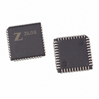
Z8927320VSG Zilog, Z8927320VSG Datasheet - Page 28

Z8927320VSG
Manufacturer Part Number
Z8927320VSG
Description
DSP 20MHZ 16-BIT W/ A/D 44-PLCC
Manufacturer
Zilog
Series
Z892x3r
Type
Fixed Pointr
Datasheet
1.Z8937320FSC00TR.pdf
(60 pages)
Specifications of Z8927320VSG
Interface
SPI, 3-Wire Serial
Clock Rate
20MHz
Non-volatile Memory
OTP (16 kB)
On-chip Ram
1kB
Voltage - I/o
5.00V
Voltage - Core
5.00V
Operating Temperature
0°C ~ 70°C
Mounting Type
Surface Mount
Package / Case
44-LCC (J-Lead)
Lead Free Status / RoHS Status
Lead free / RoHS Compliant
Available stocks
Company
Part Number
Manufacturer
Quantity
Price
Company:
Part Number:
Z8927320VSG
Manufacturer:
Zilog
Quantity:
50
REGISTERS (Continued)
Z89223/273/323/373
16-Bit Digital Signal Processors with A/D Converter
The following are not actually registers, but are read or writ-
ten in the same way as hardware registers on the chip:
BUS
the contents of the D-Bus. BUS is used for emulation only.
28
Register
BUS
Dn:b
EXTn
MPY output arithmetically
shifted right by three bits
Overflow Protection
is a read-only register which, when accessed, returns
S2
User Input UI1,UI0
0
0
0
0
1
1
1
1
(Read Only)
Negative
Overflow
Table 12. RPL Description
Carry
Zero
S1
0
0
1
1
0
0
1
1
Register Definition
D-Bus
Eight Data Pointers
External Register, 16-bit
S15 S14 S13
N
OV
Z
S0
0
1
0
1
0
1
0
1
S12
C
S11 S10
UI1
Loop Size
Figure 19. Status Register
256
128
UI0 SH3
16
32
64
2
4
8
S9
OP
S8
Dn:b
to locations in program memory which is efficient for co-
efficient addressing. The programmer decides which loca-
tion to choose from two bits in the status register and two
bits in the operand. Thus, only the lower 16 possible loca-
tions in RAM can be specified. At any one time, there are
eight usable pointers, four per bank, and the four pointers
are in consecutive locations in RAM. For example, if
S3/S4=01 in the status register, then D0:0/D1:0/D2:0/D3:0
refer to register locations 4/5/6/7 in RAM Bank 0. Note that
when the data pointers are being written to, a number is ac-
tually being loaded to Data RAM, so they can be used as a
limited method for writing to RAM.
EXTn
16-bit register addresses provided for mapping internal and
external peripherals into the address space of the processor.
Note that for external peripherals the actual register RAM
does not exist on the chip, but would exist as part of the ex-
ternal device, such as an A/D result latch. The External Ad-
dress Bus, EA2–EA0, the External Data Bus, ED15–ED0,
DS, WAIT, and RD/WR are used to access external periph-
erals.
EXT7
states for EXT0–EXT6, and is not available for accessing
an external peripheral.
S7
IE
UO1 UO0
refers to locations in RAM that can be used as a pointer
S6
is used for Register Bank Select, and to program wait
are external registers (n = 0 to 6). These are seven
S5
S4
S3
S2
RPL
S1
S0
DS000202-DSP0599
"Short Form Direct" bits
Pointer
User Output UO1, UO0
(Complemented)
Global Interrupt Enable
Ram
0 0 0
0 0 1
0 1 0
0 1 1
1 0 0
1 0 1
1 1 0
1 1 1
Loop
Size
256
128
16
32
64
ZiLOG
2
4
8


