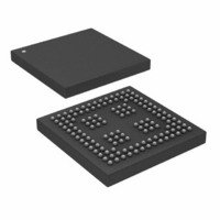
ADSP-21262SKBCZ200 Analog Devices Inc, ADSP-21262SKBCZ200 Datasheet - Page 33

ADSP-21262SKBCZ200
Manufacturer Part Number
ADSP-21262SKBCZ200
Description
IC DSP CTLR 32BIT 136CSPBGA
Manufacturer
Analog Devices Inc
Series
SHARC®r
Type
Fixed/Floating Pointr
Datasheet
1.ADSP-21262SKBCZ200.pdf
(48 pages)
Specifications of ADSP-21262SKBCZ200
Interface
DAI, SPI
Clock Rate
200MHz
Non-volatile Memory
ROM (512 kB)
On-chip Ram
256kB
Voltage - I/o
3.30V
Voltage - Core
1.20V
Operating Temperature
0°C ~ 70°C
Mounting Type
Surface Mount
Package / Case
136-CSPBGA
No. Of Bits
32 Bit
Frequency
200MHz
Supply Voltage
1.2V
Embedded Interface Type
SPI
No. Of I/o's
23
Supply Voltage Range
1.14V To 1.26V, 3.13V To 3.47V
Lead Free Status / RoHS Status
Lead free / RoHS Compliant
Other names
ADSP21262SKBCZ200
Available stocks
Company
Part Number
Manufacturer
Quantity
Price
Company:
Part Number:
ADSP-21262SKBCZ200
Manufacturer:
Analog Devices Inc
Quantity:
10 000
Part Number:
ADSP-21262SKBCZ200
Manufacturer:
ADI/亚德诺
Quantity:
20 000
Parallel Data Acquisition Port (PDAP)
The timing requirements for the PDAP are provided in
and
Channel 0 of the IDP. For details on the operation of the IDP,
see the IDP chapter of the ADSP-2126x Peripherals Manual.
Table 28. Parallel Data Acquisition Port (PDAP)
1
Parameter
Timing Requirements
t
t
t
t
t
t
Switching Characteristics
t
t
Source pins of DATA are ADDR7–0, DATA7–0, or DAI pins. Source pins for SCLK and FS are: 1) DAI pins, 2) CLKIN through PCG, or 3) DAI pins through PCG.
SPCLKEN
HPCLKEN
PDSD
PDHD
PDCLKW
PDCLK
PDHLDD
PDSTRB
Figure
24. PDAP is the parallel mode operation of
PDAP_CLKEN Setup Before PDAP_CLK Sample Edge
PDAP_CLKEN Hold After PDAP_CLK Sample Edge
PDAP_DAT Setup Before SCLK PDAP_CLK Sample Edge
PDAP_DAT Hold After SCLK PDAP_CLK Sample Edge
Clock Width
Clock Period
Delay of PDAP Strobe After Last PDAP_CLK Capture Edge for a Word
PDAP Strobe Pulse Width
(PDAP_STROBE)
(PDAP_CLKEN)
(PDAP_CLK)
DAI_P20–1
DAI_P20–1
DAI_P20–1
DATA
Figure 24. Parallel Data Acquisition Port (PDAP)
Rev. B | Page 33 of 48 | August 2005
Table 28
t
PDCLKW
SAMPLE EDGE
t
SPCLKEN
t
PDSD
1
t
PDHLDD
1
1
Note that the most significant 16 bits of external PDAP data can
be provided through either the parallel port AD15–0 or the
DAI_P20–5 pins. The remaining four bits can only be sourced
through DAI_P4–1. The timing below is valid at the
DAI_P20–1 pins or at the AD15–0 pins.
1
t
PDCLK
t
HPCLKEN
t
PDHD
t
PDSTRB
Min
2.5
2.5
2.5
2.5
7
20
2 × t
1 × t
CCLK
CCLK
– 1
Max
ADSP-21262
Unit
ns
ns
ns
ns
ns
ns
ns
ns


