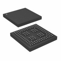
ADSP-21262SKBCZ200 Analog Devices Inc, ADSP-21262SKBCZ200 Datasheet - Page 15

ADSP-21262SKBCZ200
Manufacturer Part Number
ADSP-21262SKBCZ200
Description
IC DSP CTLR 32BIT 136CSPBGA
Manufacturer
Analog Devices Inc
Series
SHARC®r
Type
Fixed/Floating Pointr
Datasheet
1.ADSP-21262SKBCZ200.pdf
(48 pages)
Specifications of ADSP-21262SKBCZ200
Interface
DAI, SPI
Clock Rate
200MHz
Non-volatile Memory
ROM (512 kB)
On-chip Ram
256kB
Voltage - I/o
3.30V
Voltage - Core
1.20V
Operating Temperature
0°C ~ 70°C
Mounting Type
Surface Mount
Package / Case
136-CSPBGA
No. Of Bits
32 Bit
Frequency
200MHz
Supply Voltage
1.2V
Embedded Interface Type
SPI
No. Of I/o's
23
Supply Voltage Range
1.14V To 1.26V, 3.13V To 3.47V
Lead Free Status / RoHS Status
Lead free / RoHS Compliant
Other names
ADSP21262SKBCZ200
Available stocks
Company
Part Number
Manufacturer
Quantity
Price
Company:
Part Number:
ADSP-21262SKBCZ200
Manufacturer:
Analog Devices Inc
Quantity:
10 000
Part Number:
ADSP-21262SKBCZ200
Manufacturer:
ADI/亚德诺
Quantity:
20 000
ADSP-21262 SPECIFICATIONS
RECOMMENDED OPERATING CONDITIONS
1
2
3
4
5
6
ELECTRICAL CHARACTERISTICS
1
2
3
4
5
6
7
8
9
10
11
12
13
14
Parameter
V
A
V
V
V
V
V
T
T
Parameter
V
V
I
I
I
I
I
I
I
AI
C
Specifications subject to change without notice.
Applies to input and bidirectional pins: AD15–0, FLAG3–0, DAI_Px, SPICLK, MOSI, MISO, SPIDS, BOOTCFGx, CLKCFGx, RESET, TCK, TMS, TDI, TRST.
Applies to input pin CLKIN.
See
See Engineer-to-Engineer Note (No. 250) for further information.
See Engineer-to-Engineer Note (No. 216) for further information.
Specifications subject to change without notice.
Applies to output and bidirectional pins: AD15–0, RD, WR, ALE, FLAG3–0, DAI_Px, SPICLK, MOSI, MISO, EMU, TDO, CLKOUT, XTAL.
See
Applies to input pins: SPIDS, BOOTCFGx, CLKCFGx, TCK, RESET, CLKIN.
Applies to input pins with 22.5 kΩ internal pull-ups: TRST, TMS, TDI.
Applies to three-statable pins: FLAG3–0.
Applies to three-statable pins with 22.5 kΩ pull-ups: AD15–0, DAI_Px, SPICLK, MISO, MOSI.
Applies to open-drain output pins: EMU, MISO, MOSI.
Typical internal current data reflects nominal operating conditions.
IH
IL
ILPU
OZH
OZL
OZLPU
DD-INTYP
See Engineer-to-Engineer Note (No. 216) for further information.
Characterized, but not tested.
Characterized, but not tested.
Applies to all signal pins.
Guaranteed, but not tested.
DDINT
DDEXT
IH
IL
IH_CLKIN
IL_CLKIN
AMB
AMB
OH
OL
VDD
IN
DD
Thermal Characteristics on Page 39
Output Drive Currents on Page 38
B Grade (Industrial)
K Grade (Commercial)
1
1
High Level Output Voltage
Low Level Output Voltage
High Level Input Current
Low Level Input Current
Low Level Input Current Pull-Up
Three-State Leakage Current
Three-State Leakage Current
Three-State Leakage Current Pull-Up
Supply Current (Internal)
Supply Current (Analog)
Input Capacitance
Internal (Core) Supply Voltage
Analog (PLL) Supply Voltage
External (I/O) Supply Voltage
High Level Input Voltage
Low Level Input Voltage
High Level Input Voltage
Low Level Input Voltage @ V
Ambient Operating Temperature
Ambient Operating Temperature
for typical drive current capabilities.
for information on thermal specifications.
13, 14
4
12
4, 5
9, 10, 11
2
2
Rev. B | Page 15 of 48 | August 2005
6
6, 7, 8
2
2
3
@ V
@ V
@ V
5
DDEXT
DDEXT
DDEXT
DDEXT
7
4, 5
4, 6
= min
= min
= max
= max
Test Conditions
@ V
@ V
@ V
@ V
@ V
@ V
@ V
@ V
t
A
f
IN
CCLK
VDD
= 1 MHz, T
DDEXT
DDEXT
DDEXT
DDEXT
DDEXT
DDEXT
DDEXT
DDEXT
= 5.0 ns, V
= max
= min, I
= min, I
= max, V
= max, V
= max, V
= max, V
= max, V
= max, V
CASE
DDINT
OH
OL
= 25°C, V
IN
IN
IN
IN
IN
IN
= 1.0 mA
= –1.0 mA
= V
= 0 V
= 0 V
= V
= 0 V
= 0 V
= 1.2 V, T
DDEXT
DDEXT
IN
3
max
max
= 1.2 V
AMB
3
= +25°C
Min
1.14
1.14
3.13
2.0
–0.5
1.74
–0.5
–40
0
Min
2.4
ADSP-21262
Max
V
+0.8
V
+1.19
+85
+70
Max
0.4
10
10
200
10
10
200
500
10
4.7
1.26
1.26
3.47
DDEXT
DDEXT
+ 0.5 V
+ 0.5 V
Unit
V
V
V
V
V
°C
°C
Unit
V
V
µA
µA
µA
µA
µA
µA
mA
mA
pF


