AD5348BRUZ Analog Devices Inc, AD5348BRUZ Datasheet - Page 7
AD5348BRUZ
Manufacturer Part Number
AD5348BRUZ
Description
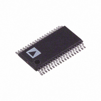
IC DAC 12BIT OCTAL VOUT 38-TSSOP
Manufacturer
Analog Devices Inc
Datasheet
1.AD5348BRUZ.pdf
(24 pages)
Specifications of AD5348BRUZ
Data Interface
Parallel
Settling Time
8µs
Number Of Bits
12
Number Of Converters
8
Voltage Supply Source
Single Supply
Power Dissipation (max)
8.3mW
Operating Temperature
-40°C ~ 105°C
Mounting Type
Surface Mount
Package / Case
38-TSSOP
Resolution (bits)
12bit
Sampling Rate
125kSPS
Input Channel Type
Parallel
Supply Voltage Range - Analog
2.5V To 5.5V
Supply Current
1mA
Digital Ic Case Style
TSSOP
Number Of Channels
8
Resolution
12b
Conversion Rate
125KSPS
Interface Type
Parallel
Single Supply Voltage (typ)
3.3/5V
Dual Supply Voltage (typ)
Not RequiredV
Architecture
Resistor-String
Power Supply Requirement
Single
Output Type
Voltage
Integral Nonlinearity Error
±16LSB
Single Supply Voltage (min)
2.5V
Single Supply Voltage (max)
5.5V
Dual Supply Voltage (min)
Not RequiredV
Dual Supply Voltage (max)
Not RequiredV
Operating Temp Range
-40C to 105C
Operating Temperature Classification
Industrial
Mounting
Surface Mount
Pin Count
38
Package Type
TSSOP
Lead Free Status / RoHS Status
Lead free / RoHS Compliant
Lead Free Status / RoHS Status
Lead free / RoHS Compliant, Lead free / RoHS Compliant
Available stocks
Company
Part Number
Manufacturer
Quantity
Price

Part Number:
AD5348BRUZ
Manufacturer:
ADI/亚德诺
Quantity:
20 000


AD5346 PIN CONFIGURATIONS AND FUNCTION DESCRIPTIONS
Table 5. AD5346 Pin Function Descriptions
TSSOP
1
2
3
4
5
6–9,
11–14
10
15,
21–24
16
17
18
19
20
25–32
33
34
35
36
37
38
Pin Number
LFCSP
35
36
37
38, 39
40
1–4,
7–10
5, 6
11,
17–20
12
13
14
15
16
21–28
29
30
31
32
33
34
Figure 5. AD5346 Pin Configuration—TSSOP
V
V
V
V
REF
V
V
V
V
V
V
REF
REF
V
AGND
DGND
V
REF
LDAC
OUT
OUT
OUT
OUT
OUT
OUT
OUT
OUT
BUF
V
GH
CD
AB
A0
A1
DD
EF
G
A
B
C
D
H
E
F
Mnemonic
V
V
V
V
V
V
AGND
DGND
BUF
LDAC
A0
A1
A2
DB
CS
RD
WR
GAIN
CLR
PD
REF
REF
REF
DD
REF
OUT
10
11
12
13
14
15
16
17
18
19
1
2
3
4
5
6
7
8
9
0
GH
EF
CD
AB
–DB
X
(Not to Scale)
AD5346
TOP VIEW
8-BIT
7
38
37
36
35
34
33
32
31
30
29
28
27
26
25
24
23
22
21
20
Function
Reference Input for DACs G and H.
Reference Input for DACs E and F.
Reference Input for DACs C and D.
Power Supply Pin(s). This part can operate from 2.5 V to 5.5 V, and the supply should be decoupled
with a 10 µF capacitor in parallel with a 0.1 µF capacitor to GND. Both V
package must be at the same potential.
Reference Input for DACs A and B.
Output of DAC X. Buffered output with rail-to-rail operation.
Analog Ground. Ground reference for analog circuitry.
Digital Ground. Ground reference for digital circuitry.
Buffer Control Pin. Controls whether the reference input to the DAC is buffered or unbuffered.
Active Low Control Input. Updates the DAC registers with the contents of the input registers, which
allows all DAC outputs to be simultaneously updated.
LSB Address Pin. Selects which DAC is to be written to.
Address Pin. Selects which DAC is to be written to.
MSB Address Pin. Selects which DAC is to be written to.
Eight Parallel Data Inputs. DB
Active Low Chip Select Input. Used in conjunction with WR to write data to the parallel interface, or
with RD to read back data from a DAC.
Active Low Read Input. Used in conjunction with CS to read data back from the internal DACs.
Active Low Write Input. Used in conjunction with CS to write data to the parallel interface.
Gain Control Pin. Controls whether the output range from the DAC is 0 V to V
Asynchronous Active Low Control Input. Clears all input registers and DAC registers to zeros.
Power-Down Pin. This active low control pin puts all DACs into power-down mode.
PD
CLR
GAIN
WR
RD
CS
DB
DB
DB
DB
DB
DB
DB
DB
DGND
DGND
DGND
DGND
A2
7
6
5
4
3
2
1
0
Rev. 0 | Page 7 of 24
7
is the MSB of these eight bits.
V
V
V
V
V
V
V
V
AGND
AGND
OUT
OUT
OUT
OUT
OUT
OUT
OUT
OUT
G
A
B
C
D
H
E
F
Figure 6. AD5346 Pin Configuration—LFCSP
10
1
2
3
4
5
6
7
8
9
40
11
12
39
13
38
AD5346/AD5347/AD5348
37
14
(Not to Scale)
AD5346
TOP VIEW
15
36
8-BIT
16
35
DD
34
17
pins on the LFCSP
18
33
REF
32
19
or 0 V to 2 × V
20
31
30
29
28
27
26
25
24
23
22
21
RD
CS
DB
DB
DB
DB
DB
DB
DB
DB
7
6
5
4
3
2
1
0
REF.
Related parts for AD5348BRUZ
Image
Part Number
Description
Manufacturer
Datasheet
Request
R

Part Number:
Description:
GSM Baseband Processing Chipset
Manufacturer:
AD [Analog Devices]
Datasheet:

Part Number:
Description:
±1.7g Dual-Axis IMEMS Accelerometer Evaluation Board
Manufacturer:
Analog Devices Inc
Datasheet:

Part Number:
Description:
Inertial Sensor Evaluation System
Manufacturer:
Analog Devices Inc
Datasheet:
Part Number:
Description:
Manufacturer:
Analog Devices Inc
Datasheet:
Part Number:
Description:
Manufacturer:
Analog Devices Inc
Datasheet:
Part Number:
Description:
Manufacturer:
Analog Devices Inc
Datasheet:
Part Number:
Description:
Manufacturer:
Analog Devices Inc
Datasheet:
Part Number:
Description:
Manufacturer:
Analog Devices Inc
Datasheet:
Part Number:
Description:
Manufacturer:
Analog Devices Inc
Datasheet:
Part Number:
Description:
Manufacturer:
Analog Devices Inc
Datasheet:
Part Number:
Description:
Manufacturer:
Analog Devices Inc
Datasheet:
Part Number:
Description:
Manufacturer:
Analog Devices Inc
Datasheet:
Part Number:
Description:
Manufacturer:
Analog Devices Inc
Datasheet: