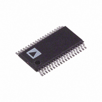
AD5348BRUZ Analog Devices Inc, AD5348BRUZ Datasheet - Page 4

AD5348BRUZ
Manufacturer Part Number
AD5348BRUZ
Description
IC DAC 12BIT OCTAL VOUT 38-TSSOP
Manufacturer
Analog Devices Inc
Datasheet
1.AD5348BRUZ.pdf
(24 pages)
Specifications of AD5348BRUZ
Data Interface
Parallel
Settling Time
8µs
Number Of Bits
12
Number Of Converters
8
Voltage Supply Source
Single Supply
Power Dissipation (max)
8.3mW
Operating Temperature
-40°C ~ 105°C
Mounting Type
Surface Mount
Package / Case
38-TSSOP
Resolution (bits)
12bit
Sampling Rate
125kSPS
Input Channel Type
Parallel
Supply Voltage Range - Analog
2.5V To 5.5V
Supply Current
1mA
Digital Ic Case Style
TSSOP
Number Of Channels
8
Resolution
12b
Conversion Rate
125KSPS
Interface Type
Parallel
Single Supply Voltage (typ)
3.3/5V
Dual Supply Voltage (typ)
Not RequiredV
Architecture
Resistor-String
Power Supply Requirement
Single
Output Type
Voltage
Integral Nonlinearity Error
±16LSB
Single Supply Voltage (min)
2.5V
Single Supply Voltage (max)
5.5V
Dual Supply Voltage (min)
Not RequiredV
Dual Supply Voltage (max)
Not RequiredV
Operating Temp Range
-40C to 105C
Operating Temperature Classification
Industrial
Mounting
Surface Mount
Pin Count
38
Package Type
TSSOP
Lead Free Status / RoHS Status
Lead free / RoHS Compliant
Lead Free Status / RoHS Status
Lead free / RoHS Compliant, Lead free / RoHS Compliant
Available stocks
Company
Part Number
Manufacturer
Quantity
Price
Part Number:
AD5348BRUZ
Manufacturer:
ADI/亚德诺
Quantity:
20 000
AD5346/AD5347/AD5348
Parameter
LOGIC OUTPUTS
POWER REQUIREMENTS
See footnotes after the AC Characteristics table.
AC CHARACTERISTICS
Table 2. V
Parameter
Output Voltage Settling Time
Slew Rate
Major Code Transition Glitch
Energy
Digital Feedthrough
Digital Crosstalk
Analog Crosstalk
DAC-to-DAC Crosstalk
Multiplying Bandwidth
Total Harmonic Distortion
1
2
3
4
5
6
7
Temperature range: B Version: –40°C to +105°C; typical specifications are at 25°C.
See Terminology section.
Linearity is tested using a reduced code range: AD5346 (Code 8 to 255); AD5347 (Code 28 to 1023); AD5348 (Code 115 to 4095).
DC specifications tested with outputs unloaded.
This corresponds to x codes. x = deadband voltage/LSB size.
Guaranteed by design and characterization, not production tested.
For the amplifier output to reach its minimum voltage, offset error must be negative. For the amplifier output to reach its maximum voltage, V
the offset plus gain error must be positive.
V
V
V
I
I
AD5346
AD5347
AD5348
DD
DD
DD
DD
DD
Output Low Voltage, V
Output High Voltage, V
Output Low Voltage, V
Output High Voltage, V
V
V
V
V
(Normal Mode)
(Power-Down Mode)
DD
DD
DD
DD
= 4.5 V to 5.5 V
= 2.5 V to 3.6 V
= 4.5 V to 5.5 V
= 2.5 V to 3.6 V
= 4.5 V to 5.5 V
= 2.5 V to 3.6 V
DD
2
2
= 2.5 V to 5.5 V; R
6
OL
OL
OH
OH
L
= 2 kΩ to GND; C
Min
V
V
2.5
6
Min
DD
DD
– 1
– 0.5
TO OUTPUT
B Version
Typ
6
7
8
0.5
3.5
200
0.7
8
1
1
–70
B Version
Figure 2. Load Circuit for Digital Output Timing Specifications
Typ
1
0.8
0.4
0.12
PIN
1
50pF
1
L
Max
0.4
0.4
5.5
1.65
1.4
1
1
C
Max
8
9
10
= 200 pF to GND; all specifications T
L
Rev. 0 | Page 4 of 24
200µA
200µA
Unit
V
V
V
V
V
mA
mA
µA
µA
Unit
µs
µs
µs
V/µs
nV-s
nV-s
nV-s
nV-s
nV-s
kHz
dB
I
I
OL
OH
Conditions/Comments
I
I
I
I
All DACs in unbuffered mode. In buffered mode,
extra current is typically x µA per DAC, where x = 5 µA +
V
V
Conditions/Comments
1/4 scale to 3/4 scale change (40 H to C0 H)
1/4 scale to 3/4 scale change (100 H to 300 H)
1/4 scale to 3/4 scale change (400 H to C00 H)
1 LSB change around major carry
V
V
V
V
SINK
SOURCE
SINK
SOURCE
V
IH
REF
IH
REF
REF
REF
OH
= V
= V
/R
(min) + V
= 200 µA
= 200 µA
= 2. V ±0.1 V p-p; frequency = 10 kHz; unbuffered mode
= 2 V
= 2 V ±0.1 V p-p; unbuffered mode
DAC
= 200 µA
= 200 µA
DD
DD
2
, V
, V
OL
IL
IL
= GND
= GND
(max)
MIN
to T
MAX
, unless otherwise noted
REF
= V
DD
and


