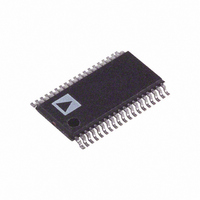
AD5348BRUZ Analog Devices Inc, AD5348BRUZ Datasheet - Page 16

AD5348BRUZ
Manufacturer Part Number
AD5348BRUZ
Description
IC DAC 12BIT OCTAL VOUT 38-TSSOP
Manufacturer
Analog Devices Inc
Datasheet
1.AD5348BRUZ.pdf
(24 pages)
Specifications of AD5348BRUZ
Data Interface
Parallel
Settling Time
8µs
Number Of Bits
12
Number Of Converters
8
Voltage Supply Source
Single Supply
Power Dissipation (max)
8.3mW
Operating Temperature
-40°C ~ 105°C
Mounting Type
Surface Mount
Package / Case
38-TSSOP
Resolution (bits)
12bit
Sampling Rate
125kSPS
Input Channel Type
Parallel
Supply Voltage Range - Analog
2.5V To 5.5V
Supply Current
1mA
Digital Ic Case Style
TSSOP
Number Of Channels
8
Resolution
12b
Conversion Rate
125KSPS
Interface Type
Parallel
Single Supply Voltage (typ)
3.3/5V
Dual Supply Voltage (typ)
Not RequiredV
Architecture
Resistor-String
Power Supply Requirement
Single
Output Type
Voltage
Integral Nonlinearity Error
±16LSB
Single Supply Voltage (min)
2.5V
Single Supply Voltage (max)
5.5V
Dual Supply Voltage (min)
Not RequiredV
Dual Supply Voltage (max)
Not RequiredV
Operating Temp Range
-40C to 105C
Operating Temperature Classification
Industrial
Mounting
Surface Mount
Pin Count
38
Package Type
TSSOP
Lead Free Status / RoHS Status
Lead free / RoHS Compliant
Lead Free Status / RoHS Status
Lead free / RoHS Compliant, Lead free / RoHS Compliant
Available stocks
Company
Part Number
Manufacturer
Quantity
Price
Part Number:
AD5348BRUZ
Manufacturer:
ADI/亚德诺
Quantity:
20 000
AD5346/AD5347/AD5348
FUNCTIONAL DESCRIPTION
The AD5346/AD5347/AD5348 are octal resistor-string DACs
fabricated by a CMOS process with resolutions of 8, 10, and 12
bits, respectively. They are written to using a parallel interface.
They operate from single supplies of 2.5 V to 5.5 V, and the
output buffer amplifiers offer rail-to-rail output swing. The gain
of the buffer amplifiers can be set to 1 or 2 to give an output
voltage range of 0 V to V
AD5347/AD5348 have reference inputs that may be buffered to
draw virtually no current from the reference source. The devices
have a power-down feature that reduces current consumption
to only 100 nA @ 3 V.
DIGITAL-TO-ANALOG SECTION
The architecture of one DAC channel consists of a reference
buffer and a resistor-string DAC followed by an output buffer
amplifier. The voltage at the V
voltage for the DAC. Figure 37 shows a block diagram of the
DAC architecture. Because the input coding to the DAC is
straight binary, the ideal output voltage is given by
where:
D is the decimal equivalent of the binary code, which is loaded
to the DAC register:
N is the DAC resolution.
Gain is the output amplifier gain (1 or 2).
RESISTOR STRING
The resistor string section is shown in Figure 38. It is simply a
string of resistors, each of value R. The digital code loaded to
the DAC register determines at what node on the string the
voltage is tapped off to be fed into the output amplifier. The
voltage is tapped off by closing one of the switches connecting
the string to the amplifier. Because it is a string of resistors, it is
guaranteed monotonic.
REGISTER
INPUT
V
0–255 for AD5346 (8 bits)
0–1023 for AD5347 (10 bits)
0–4095 for AD5348 (12 bits)
OUT
=
V
REF
Figure 37. Single DAC Channel Architecture
×
REGISTER
2
D
BUF
DAC
N
×
Gain
REF
or 0 V to 2 × V
REF
RESISTOR
STRING
pin provides the reference
V
REF
AB
REFERENCE
BUFFER
REF.
BUFFER AMPLIFIER
(GAIN = +1 OR +2)
The AD5346/
OUTPUT
V
OUT
Rev. 0 | Page 16 of 24
A
DAC REFERENCE INPUT
The DACs operate with an external reference. The AD5346/
AD5347/AD5348 have a reference input for each pair of DACs.
The reference inputs may be configured as buffered or
unbuffered. This option is controlled by the BUF pin.
In buffered mode (BUF = 1), the current drawn from an
external reference voltage is virtually zero because the imped-
ance is at least 10 MΩ. The reference input range is 1 V to V
In unbuffered mode (BUF = 0), the user can have a reference
voltage as low as 0.25 V and as high as V
restriction due to headroom and footroom of the reference
amplifier. The impedance is still large at typically 90 kΩ for 0 V
to V
If using an external buffered reference (such as REF192), there
is no need to use the on-chip buffer.
OUTPUT AMPLIFIER
The output buffer amplifier is capable of generating output
voltages to within 1 mV of either rail. Its actual range depends
on V
If a gain of +1 is selected (GAIN = 0), the output range is
0.001 V to V
If a gain of +2 is selected (GAIN = +1), the output range is
0.001 V to 2 × V
maximum output is limited to V
The output amplifier is capable of driving a load of 2 kΩ to
GND or V
and sink capabilities of the output amplifier can be seen in
Figure 24.
The slew rate is 0.7 V/µs with a half-scale settling time to ±0.5 LSB
(at 8 bits) of 6 s with the output unloaded. See Figure 29.
REF
REF
mode and 45 kΩ for 0 V to 2 × V
, GAIN, the load on V
DD
REF
, in parallel with 500 pF to GND or V
.
REF
R
R
R
R
R
. However, because of clamping, the
Figure 38. Resistor String
V
REF
OUT
, and offset error.
DD
– 0.001 V.
TO OUTPUT
AMPLIFIER
DD
REF
because there is no
mode.
DD
. The source
DD
.


