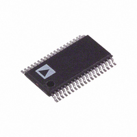
AD5348BRUZ Analog Devices Inc, AD5348BRUZ Datasheet - Page 21

AD5348BRUZ
Manufacturer Part Number
AD5348BRUZ
Description
IC DAC 12BIT OCTAL VOUT 38-TSSOP
Manufacturer
Analog Devices Inc
Datasheet
1.AD5348BRUZ.pdf
(24 pages)
Specifications of AD5348BRUZ
Data Interface
Parallel
Settling Time
8µs
Number Of Bits
12
Number Of Converters
8
Voltage Supply Source
Single Supply
Power Dissipation (max)
8.3mW
Operating Temperature
-40°C ~ 105°C
Mounting Type
Surface Mount
Package / Case
38-TSSOP
Resolution (bits)
12bit
Sampling Rate
125kSPS
Input Channel Type
Parallel
Supply Voltage Range - Analog
2.5V To 5.5V
Supply Current
1mA
Digital Ic Case Style
TSSOP
Number Of Channels
8
Resolution
12b
Conversion Rate
125KSPS
Interface Type
Parallel
Single Supply Voltage (typ)
3.3/5V
Dual Supply Voltage (typ)
Not RequiredV
Architecture
Resistor-String
Power Supply Requirement
Single
Output Type
Voltage
Integral Nonlinearity Error
±16LSB
Single Supply Voltage (min)
2.5V
Single Supply Voltage (max)
5.5V
Dual Supply Voltage (min)
Not RequiredV
Dual Supply Voltage (max)
Not RequiredV
Operating Temp Range
-40C to 105C
Operating Temperature Classification
Industrial
Mounting
Surface Mount
Pin Count
38
Package Type
TSSOP
Lead Free Status / RoHS Status
Lead free / RoHS Compliant
Lead Free Status / RoHS Status
Lead free / RoHS Compliant, Lead free / RoHS Compliant
Available stocks
Company
Part Number
Manufacturer
Quantity
Price
Part Number:
AD5348BRUZ
Manufacturer:
ADI/亚德诺
Quantity:
20 000
COARSE AND FINE ADJUSTMENT USING
THE AD5346/AD5347/AD5348
Two of the DACs in the AD5346/AD5347/AD5348 can be
paired together to form a coarse and fine adjustment function,
as shown in Figure 47. As with the window comparator
previously described, the description refers to DACs A and B.
DAC A provides the coarse adjustment, while DAC B provides
the fine adjustment. Varying the ratio of R1 and R2 changes the
relative effect of the coarse and fine adjustments. With the
resistor values shown, the output amplifier has unity gain for
the DAC A output, so the output range is 0 V to (V
For DAC B, the amplifier has a gain of 7.6 × 10
a range equal to 2 LSBs of DAC A.
The circuit is shown with a 2.5 V reference, but reference
voltages up to V
rail-to-rail output swing.
AD780/ADR381/REF192
EXT
REF
WITH V
GND
V
IN
V
OUT
DD
= 5V
DD
Figure 47. Coarse and Fine Adjustment
0.1µF
0.1µF
may be used. The op amps indicated allow a
V
AD5346/AD5347/
REF
10µF
AB
AD5348
V
GND
DD
V
DD
= 5V
V
V
OUT
OUT
A
B
390Ω
R4
51.2kΩ
390Ω
R1
R2
–3
, giving DAC B
51.2kΩ
R3
REF
5V
– 1 LSB).
V
Rev. 0 | Page 21 of 24
OUT
POWER SUPPLY BYPASSING AND GROUNDING
In any circuit where accuracy is important, careful consideration
of the power supply and ground return layout helps to ensure
the rated performance.
The printed circuit board on which the AD5346/AD5347/
AD5348 is mounted should be designed so that the analog and
digital sections are separated and are confined to certain areas
of the board. This facilitates the use of ground planes that can
be separated easily. A minimum etch technique is generally best
for ground planes because it gives the best shielding. Digital and
analog ground planes should be joined in one place only. If the
AD5346/AD5347/AD5348 is the only device requiring an
AGND-to-DGND connection, then the ground planes should
be connected at the AGND and DGND pins of the AD5346/
AD5347/AD5348. If the AD5346/AD5347/AD5348 is in a
system where multiple devices require AGND-to-DGND
connections, the connection should be made at one point only, a
star ground point that should be established as close as possible
to the AD5346/AD5347/AD5348.
The AD5346/AD5347/AD5348 should have ample supply
bypassing of 10 µF in parallel with 0.1 µF on the supply located
as close to the package as possible, ideally right up against the
device. The 10 µF capacitors are the tantalum bead type. The
0.1 µF capacitor should have low effective series resistance
(ESR) and effective series inductance (ESI), such as the
common ceramic types that provide a low impedance path to
ground at high frequencies to handle transient currents due to
internal logic switching.
The power supply lines of the device should use the largest trace
possible to provide low impedance paths and to reduce the
effects of glitches on the power supply line. Fast switching
signals such as clocks should be shielded with digital ground to
avoid radiating noise to other parts of the board, and should
never be run near the reference inputs. Avoid crossover of
digital and analog signals. Traces on opposite sides of the board
should run at right angles to each other to reduce the effects of
feedthrough through the board. A microstrip technique is by far
the best, but not always possible with a double-sided board. In
this technique, the component side of the board is dedicated to
ground plane, while signal traces are placed on the solder side.
AD5346/AD5347/AD5348


