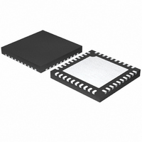
MAX11043ATL+ Maxim Integrated Products, MAX11043ATL+ Datasheet - Page 19

MAX11043ATL+
Manufacturer Part Number
MAX11043ATL+
Description
IC ADC 16BIT W/DAC 40-TQFN-EP
Manufacturer
Maxim Integrated Products
Type
ADC, DACr
Datasheet
1.MAX11043ATL.pdf
(33 pages)
Specifications of MAX11043ATL+
Resolution (bits)
16 b
Sampling Rate (per Second)
9.6M
Data Interface
Serial
Voltage Supply Source
Analog and Digital
Voltage - Supply
3 V ~ 3.6 V
Operating Temperature
-40°C ~ 125°C
Mounting Type
Surface Mount
Package / Case
40-TQFN Exposed Pad
Number Of Converters
4
Conversion Rate
1600 KSPs
Resolution
16 bit
Interface Type
SPI
Voltage Reference
2.5 V
Supply Voltage (max)
3.6 V
Supply Voltage (min)
3 V
Maximum Power Dissipation
2963 mW
Maximum Operating Temperature
+ 125 C
Mounting Style
SMD/SMT
Input Voltage
3.3 V
Minimum Operating Temperature
- 40 C
Lead Free Status / RoHS Status
Lead free / RoHS Compliant
The ADC channel A, B, C, and D result registers pro-
vide the result data from the 4 ADC channels. EOC
asserts low when new data is available. Initiate a data
read prior to the next rising edge of EOC or the result is
overwritten. Set bit 5 of the configuration register 08h
high to read the data out in 24-bit resolution or set bit 5
low to read the data out in 16-bit resolution.
Status Register (07h)
The status register contains the channel overflow flags
and POR bits.
X<7:6>: Don’t-care bits.
Flash Busy<5>: Do not start a new flash operation until
this is 0.
Configuration Register (08h)
EXTCLK<15>: External clock select.
1 = logic-level clock supplied on OSCIN.
0 = crystal or resonator connected between OSCIN
and OSCOUT (default).
CLKDIV1:CLKDIV0<14:13>: Clock divider ratio (EX
clock : ADC sample clock).
00 = 1:2 clock divider.
01 = 1:3 clock divider.
10 = 1:4 clock divider.
11 = 1:6 clock divider (default).
PD<12>: Power-down analog circuitry (reference and
SPI interface remains active).
1 = low-power mode.
0 = normal operation (default).
EXTCLK
PDDAC
BIT 15
BIT 7
4-Channel, 16-Bit, Simultaneous-Sampling ADCs
BIT 7
X
with PGA, Filter, and 8-/12-Bit Dual-Stage DAC
CLKDIV1
______________________________________________________________________________________
PDOSC
BIT 14
BIT 6
BIT 6
X
ADCA, ADCB, ADCC, and ADCD
Result Registers (00h–03h)
Register Functions
Flash Busy
CLKDIV0
BIT 13
BIT 5
24BIT
BIT 5
SCHANA
BIT 12
BOOT
BIT 4
BIT 4
PD
Registers ADCAB, ADCCD, and ADCABCD contain
concatenated ADC results ensuring simultaneous
results are read. This reduces the risk of reading sam-
ples delayed by one cycle from channel to channel.
Set bit 5 of the configuration register 08h high to read
the data out in 24-bit resolution or set bit 5 low to read
the data out in 16-bit resolution.
BOOT<4>: Power-on reset flag.
OFLG_<3:0>: Channel overflow flag, one per channel.
PD_<11:8>: ADC power-down for each channel (A, B,
C, and D).
1 = powers down analog signal path.
0 = normal operation (default).
PDDAC< 7>: DAC power-down.
1 = fine DAC buffer powered down.
0 = normal operation (default).
PDOSC<6>: Oscillator power-down.
1 = oscillator powered down (disconnects EX clock in
EX clock mode).
0 = normal operation (default).
24BIT<5>: ADC output data format.
1 = ADC data output as 24 bits.
0 = ADC data output as 16 bits (default).
Use the 24-bit ADC output in conjunction with external
digital filtering to improve signal-to-noise ratio.
SCHANB
OFLGA
BIT 11
BIT 3
BIT 3
PDA
SCHANC
OFLGB
BIT 10
BIT 2
BIT 2
PDB
ADCAB, ADCCD, and ADCABCD
Result Registers (04h–06h)
SCHAND
OFLGC
BIT 1
BIT 9
BIT 1
PDC
DECSEL
OFLGD
BIT 0
BIT 8
BIT 0
PDD
19


