AD7156BCPZ-REEL7 Analog Devices Inc, AD7156BCPZ-REEL7 Datasheet - Page 7
AD7156BCPZ-REEL7
Manufacturer Part Number
AD7156BCPZ-REEL7
Description
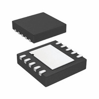
IC CDC 2CH 12BIT 1.8V 10LFCSP
Manufacturer
Analog Devices Inc
Type
Capacitance-to-Digital Converterr
Datasheet
1.AD7156BCPZ-REEL7.pdf
(28 pages)
Specifications of AD7156BCPZ-REEL7
Resolution (bits)
12 b
Data Interface
Serial
Sampling Rate (per Second)
100k
Voltage Supply Source
Single Supply
Voltage - Supply
1.8 V ~ 3.6 V
Operating Temperature
-40°C ~ 85°C
Mounting Type
Surface Mount
Package / Case
10-LFCSP
Sampling Rate
100SPS
Input Channel Type
Single Ended
Supply Voltage Range - Analog
1.8V To 3.6V
Supply Current
70µA
Lead Free Status / RoHS Status
Lead free / RoHS Compliant
Lead Free Status / RoHS Status
Lead free / RoHS Compliant, Lead free / RoHS Compliant
Other names
AD7156BCPZ-REEL7TR


PIN CONFIGURATION AND FUNCTION DESCRIPTIONS
Table 4. Pin Function Descriptions
Pin No.
1
2
3
4
5
6
7
8
9
10
Mnemonic
GND
VDD
CIN2
CIN1
EXC2
EXC1
OUT2
SCL
OUT1
SDA
Description
Ground Pin.
Power Supply Voltage. This pin should be decoupled to GND using a low impedance capacitor, such as a
0.1 μF X7R multilayer ceramic capacitor.
CDC Capacitive Input Channel 2. The measured capacitance (sensor) is connected between the EXC2 pin and
the CIN2 pin. If not used, this pin can be left open circuit or be connected to GND. When a conversion is
performed on Channel 2, the CIN2 pin is internally connected to a high impedance input of the Σ-Δ
modulator. When a conversion is performed on the other channel or in idle mode
the CIN2 pin is internally disconnected and left floating by the part.
CDC Capacitive Input Channel 1. The measured capacitance (sensor) is connected between the EXC1 pin and
the CIN1 pin. If not used, this pin can be left open circuit or be connected to GND. When a conversion is
performed on Channel 1, the CIN1 pin is internally connected to a high impedance input of the Σ-Δ
modulator. When a conversion is performed on the other channel or in idle mode
the CIN1 pin is internally disconnected and left floating by the part.
CDC Excitation Output Channel 2. The measured capacitance is connected between the EXC2 pin and the
CIN2 pin. If not used, this pin should be left as an open circuit. When a conversion is performed on Channel 2,
the EXC2 pin is internally connected to the output of the excitation signal driver. When a conversion is per-
formed on the other channel or in idle mode or power-
to GND.
CDC Excitation Output Channel 1. The measured capacitance is connected between the EXC1 pin and the
CIN1 pin. If not used, this pin should be left as an open circuit. When a conversion is performed on Channel 1,
the EXC1 pin is internally connected to the output of the excitation signal driver. When a conversion is per-
formed on the other channel or in idle mode or power-
to GND.
Logic Output Channel 1. A high level on this output indicates proximity detected on CIN1.
Logic Output Channel 2. A high level on this output indicates proximity detected on CIN2.
Serial Interface Clock Input. This pin connects to the master clock line and requires a pull-up resistor if not
provided elsewhere in the system.
Serial Interface Bidirectional Data. This pin connects to the master data line and requires a pull-up resistor if
not provided elsewhere in the system.
NOTES
1. THE EXPOSED PAD MUST BE CONNECTED TO
GND OR IT MUST BE ISOLATED (FLOATING).
EXC2
CIN2
CIN1
GND
VDD
Figure 3. Pin Configuration
1
2
3
4
5
Rev. 0 | Page 7 of 28
(Not to Scale)
AD7156
TOP VIEW
10
9
8
7
6
SDA
SCL
OUT2
OUT1
EXC1
down mode, the EXC2 pin is internally connected
down mode, the EXC1 pin is internally connected
or power-down mode,
or power-down mode,
AD7156
Related parts for AD7156BCPZ-REEL7
Image
Part Number
Description
Manufacturer
Datasheet
Request
R

Part Number:
Description:
1.8V 2-ch Capactive Prom Swit ITF OTH IC
Manufacturer:
Analog Devices Inc
Datasheet:

Part Number:
Description:
±1.7g Dual-Axis IMEMS Accelerometer Evaluation Board
Manufacturer:
Analog Devices Inc
Datasheet:

Part Number:
Description:
Inertial Sensor Evaluation System
Manufacturer:
Analog Devices Inc
Datasheet:
Part Number:
Description:
Manufacturer:
Analog Devices Inc
Datasheet:
Part Number:
Description:
Manufacturer:
Analog Devices Inc
Datasheet:
Part Number:
Description:
Manufacturer:
Analog Devices Inc
Datasheet:
Part Number:
Description:
Manufacturer:
Analog Devices Inc
Datasheet:
Part Number:
Description:
Manufacturer:
Analog Devices Inc
Datasheet:
Part Number:
Description:
Manufacturer:
Analog Devices Inc
Datasheet:
Part Number:
Description:
Manufacturer:
Analog Devices Inc
Datasheet:
Part Number:
Description:
Manufacturer:
Analog Devices Inc
Datasheet:
Part Number:
Description:
Manufacturer:
Analog Devices Inc
Datasheet:
Part Number:
Description:
Manufacturer:
Analog Devices Inc
Datasheet: