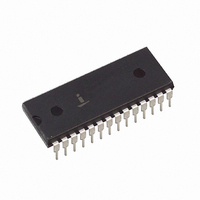
HI3-7159A-5 Intersil, HI3-7159A-5 Datasheet - Page 8

HI3-7159A-5
Manufacturer Part Number
HI3-7159A-5
Description
CONV A/D 5.5 DIGITIC MPU 28-DIP
Manufacturer
Intersil
Datasheet
1.HI3-7159A-5.pdf
(14 pages)
Specifications of HI3-7159A-5
Number Of Bits
8
Sampling Rate (per Second)
200k
Data Interface
Serial, Parallel
Number Of Converters
1
Voltage Supply Source
Analog and Digital, Dual ±
Operating Temperature
0°C ~ 70°C
Mounting Type
Through Hole
Package / Case
28-DIP (0.600", 15.24mm)
Lead Free Status / RoHS Status
Contains lead / RoHS non-compliant
Available stocks
Company
Part Number
Manufacturer
Quantity
Price
Serial Mode 2
Serial Mode 2 is selected by tying SEL (pin 28) low, SMS0
(pin 18) high, and SMS1 (pin 19) low, as shown in Figure 4C.
This mode of operation is identical to Serial Mode 1, except
that each device now has one of 32 unique addresses
determined by the state of pins 20-23 and 17, as shown in
Table 3. This allows multiple HI-7159As to be attached to the
same pair of serial lines.
When the microprocessor sends out an Address Byte (Table
4) that matches one of the HI-7159As’ hardwired addresses,
that particular HI-7159A is selected for all further I/O until
another Address Byte with a different address is
transmitted.
Reading the HI-7159A
Despite the wide variety of interface options available on the
HI-7159A, the procedure for communicating with it is
essentially the same in all four modes. (Serial Mode 2 differs
from the rest in two respects: the chip to be communicated
with must first be sent an address byte to select it, and the
digit bytes are sent one by one, for a total of six bytes,
instead of in pairs.) There are two types of bytes that can be
sent to the converter, commands and requests. A command
byte (Table 5) sets the parameters of and initiates a
conversion. Those parameters are: continuity of the
conversion (single or continuous), resolution (5
TABLE 3. HARDWARE ADDRESS SELECTION FOR MODE 2
B4 (MSB)
D7
PIN 17
ADDRESS BIT
0
D7
0
(RESERVED)
D7
1
D6
0
PIN 23
D6
(RESERVED)
0
B3
D5
0
TABLE 6. REQUEST BYTE FORMAT, PARALLEL AND SERIAL MODE 1 (SENT TO HI-7159A)
Single
Continuous
D6
0
D5
PIN 22
0
(RESERVED)
B2
TABLE 4. SERIAL MODE 2 ADDRESS BYTE FORMAT (SENT TO HI-7159A)
8
CONTINUITY
TABLE 5. COMMAND BYTE FORMAT (SENT TO HI-7159A)
D4
0
PIN 21
D5
0
B1
Digit Pair 0, 1
Digit Pair 2, 3
Digit Pair 4, 5
Converter Status
D4
0
1
1
/
2
B0 (LSB)
or 4
PIN 20
5
4
1
1
(MSB)
/
/
2
2
1
D4
/
B4
2
RESOLUTION
HI-7159A
BYTE REQUEST
digits), and type of conversion (Compensated,
Uncompensated, or Error Only). Bit D0 = 0 indicates that this
is a command byte and a new conversion(s) should be
started.
A request byte (Table 6) asks for either the status of the
converter or the result of a conversion. All bits of a request
should be set to 0 except D3, D2, and D0. D3 and D2
determine the type of request (status or digit pair), and D0 =
1 indicates to the HI-7159A that this is a request byte. Serial
Mode 2 uses a slightly modified request byte, shown in Table
7, allowing it to individually select each of the six digit bytes.
Upon receipt of a request, the HI-7159A will respond with
either a status or a digit byte. The status byte (Table 8)
returns the current state of the converter. Bit D6 = 1
indicates that a new conversion has been completed since
the last time the status byte was read. Bit D6 is cleared after
it is read. Bit D4 shows the current continuity (single or
continuous). Bit D3 indicates the resolution (5
digits) of the conversion, and bits D2 and D1 indicate the
type (Compensated, Uncompensated, or Error Only). Bit
D0 = 0 indicates that there was no parity error detected in
the last request byte.
The three digit bytes (Table 9) each contain two nibbles
representing two digits of the conversion. The sixth nibble
contains the MSD (most significant digit), polarity
(1 = positive) and overrange (1 = overrange) information. In
Serial Mode 2 the digits (Table 10) are requested and
received individually, so a total of six requests and six reads
is necessary to obtain all 5
D3
B3
D3
1
0
D3
0
0
1
1
Comp
Uncomp
Error Only
CONVERSION TYPE
D2
0
1
0
1
D2
B2
(RESERVED)
D2
1
1
1
0
/
2
digits.
D1
0
D1
D1
B1
1
0
1
COMMAND BIT
REQUEST BIT
1
/
2
D0
or 4
0
(LSB)
D0
1
D0
B0
1
/
2


