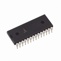
HI3-7159A-5 Intersil, HI3-7159A-5 Datasheet - Page 12

HI3-7159A-5
Manufacturer Part Number
HI3-7159A-5
Description
CONV A/D 5.5 DIGITIC MPU 28-DIP
Manufacturer
Intersil
Datasheet
1.HI3-7159A-5.pdf
(14 pages)
Specifications of HI3-7159A-5
Number Of Bits
8
Sampling Rate (per Second)
200k
Data Interface
Serial, Parallel
Number Of Converters
1
Voltage Supply Source
Analog and Digital, Dual ±
Operating Temperature
0°C ~ 70°C
Mounting Type
Through Hole
Package / Case
28-DIP (0.600", 15.24mm)
Lead Free Status / RoHS Status
Contains lead / RoHS non-compliant
Available stocks
Company
Part Number
Manufacturer
Quantity
Price
Therefore values of R
400k . The exact value of R
exact integrator swing desired after choosing a standard
capacitor value for C
The most critical component in any integrating A/D converter
is the integrating capacitor, C
resolution, it is imperative that this component perform as
closely to an ideal capacitor as possible. Any amount of
leakage or dielectric absorption will manifest itself as
linearity errors. For this reason C
polypropylene capacitor. Use of any other type may degrade
performance. The value of C
magnitude of the desired maximum integrator output voltage
swing as shown below:
V
Solving for C
where V
integrator, V
to the converter (equal to 2 X V
which V
the maximum integrator output voltage is made as large as
possible, yet still less than the nonlinear region in the vicinity
of the power supply limit. A full scale output swing of about
3V provides the greatest accuracy and linearity.
NOTE: The integrator is auto-zeroed to the voltage at V
LO
| less headroom for positive input voltages (inputs where V
HI
grator will have | V
(inputs where V
or near A
tions where V
should be included in the integrator swing considerations. The follow-
ing formula combines all the above considerations:.
Gain Error Adjustments
While the HI-7159A has a very linear transfer characteristic
in both the positive and negative directions, the slope of the
line is slightly greater for negative inputs than for positive.
This results in the transfer characteristic shown in Figure 9.
One end point of this curve, typically the positive side, can
be adjusted to zero error by trimming the reference voltage.
The other (negative) side will have a fixed gain error. This
error can be removed in software by multiplying all negative
readings by a scale factor, determined by dividing the ideal
full scale reading (-200,000 counts) by the actual full scale
reading when V
C
V
SWING
INT
- V
IN LO
is negative with respect to A
IN LO
=
–
IN
---------------------------------------------- -
SWING
GND
=
R
---------------------------------------------------------------------- -
> 0). If V
V
INT
is integrated. The best results are achieved when
-------------------------------------
IN HI
R
V
IN
IN LO
R
and the above equations will be adequate. In applica-
INT
V
IN
INT
IN HI
INT
IN
is the full scale input voltage (V
V
IN
is the maximum output voltage swing of the
IN LO
–
yields:
t
SWING
may be more than 0.1V away from A
INT
V
IN LO
t
C
= -2.00000V.
INT
- V
C
IN LO
INT
INT
INT
IN LO
INT
| less headroom for negative input voltages
is positive with respect to A
.
f
should be between 200k and
10 000
OSC
< 0). In most applications V
GND
INT
INT
12
INT
REF
, the integrator will have | V
may be altered to get the
. For a converter of this
is determined by the
INT
), and t
3V
must be a high quality
INT
IN HI
is the time in
GND
IN LO
GND
- V
IN LO
, the inte-
IN
IN LO
, it
. If
IN LO
is at
VIN
HI-7159A
)
C
Depending on the polarity of the input signal, either the
negative or the positive terminal of the reference capacitor
will be connected to A
reference deintegration. In systems where V
to analog ground, the reference capacitor is effectively
shifted down by | V
not shifted at all for negative input voltages. This shift can
cause some charge on the reference capacitor to be lost
due to stray capacitance between the reference capacitor
leads and ground traces or other fixed potentials on the
board. The reference voltage will now be slightly smaller for
positive inputs. This difference in reference voltages for
positive and negative inputs appears as rollover error.
The HI-7159A provides two guard ring outputs to minimize
this effect. Each guard ring output is a buffered version of the
voltage at its respective C
C
corresponding guard rings, no charge will be lost as C
moved. Figure 10 shows two slightly different patterns. The
first one is for capacitors of symmetrical construction, the
second is for capacitors with outside foils (one end of the
capacitor is the entire outside.
FIGURE 9. TYPICAL HI-7159A TRANSFER CHARACTERISTIC
-200,012
COUNTS
REF
REF
pins and under C
Guard Pins
FIGURE 10. TYPICAL GUARD RING LAYOUT
-2
-1
REF
GND
REF
| for positive input voltages, and is
INPUT (V)
REF
to provide the correct polarity for
0
itself are surrounded by their
(5)
(6)
(7)
(8)
(5)
(6)
(7)
(8)
pin. If the traces going to the
C
C
C
C
C
C
C
C
REF
REF
REF
REF
REF
REF
REF
REF
1
-
-
+
+
-
-
+
+ GUARD
GUARD
GUARD
GUARD
HI -7159A
HI -7159A
REF LO
2
200,000
100,000
000,000
-100,000
-200,000
is tied
REF
is


