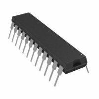
AD7712AN Analog Devices Inc, AD7712AN Datasheet - Page 6

AD7712AN
Manufacturer Part Number
AD7712AN
Description
IC ADC SIGNAL COND LC2MOS 24-DIP
Manufacturer
Analog Devices Inc
Datasheet
1.AD7712ARZ.pdf
(28 pages)
Specifications of AD7712AN
Data Interface
Serial
Rohs Status
RoHS non-compliant
Number Of Bits
24
Sampling Rate (per Second)
1.03k
Number Of Converters
1
Power Dissipation (max)
45mW
Voltage Supply Source
Analog and Digital, Dual ±
Operating Temperature
-40°C ~ 85°C
Mounting Type
Through Hole
Package / Case
24-DIP (0.300", 7.62mm)
Resolution (bits)
24bit
Sampling Rate
1.028kSPS
Input Channel Type
Differential
Supply Voltage Range - Digital
4.75V To 5.25V
Supply Current
4.5mA
Lead Free Status / RoHS Status
Contains lead / RoHS non-compliant
Available stocks
Company
Part Number
Manufacturer
Quantity
Price
Part Number:
AD7712AN
Manufacturer:
ADI/亚德诺
Quantity:
20 000
Company:
Part Number:
AD7712ANZ
Manufacturer:
ALTERA
Quantity:
300
AD7712
TIMING CHARACTERISTICS
Parameter
External Clocking Mode
NOTES
8
Specifications subject to change without notice.
These numbers are derived from the measured time taken by the data output to change 0.5 V when loaded with the circuit of Figure 1. The measured number
is then extrapolated back to remove effects of charging or discharging the 100 pF capacitor. This means that the times quoted in the timing characteristics are
the true bus relinquish times of the part and, as such, are independent of external bus loading capacitances.
f
SCLK
t
t
t
t
t
t
t
t
t
t
t
t
t
t
t
t
t
20
21
22
23
24
25
26
27
28
29
30
31
32
33
34
35
36
7
7
8
8
Figure 1. Load Circuit for Access Time and
Bus Relinquish Time
TO OUTPUT
PIN
100pF
Limit at T
(A, S Versions)
f
0
0
2
0
4
10
2
2
2
t
10
t
10
5
0
0
4
2
30
CLK IN
CLK IN
CLK IN
t
t
t
t
t
t
t
t
CLK IN
CLK IN
CLK IN
CLK IN
CLK IN
CLK IN
CLK IN
CLK IN
200 A
1.6mA
/5
+ 10
+ 10
(continued)
/2 + 50
MIN
+ 20
– SCLK High
, T
MAX
2.1V
Unit
MHz max
ns min
ns min
ns min
ns min
ns max
ns min
ns max
ns min
ns min
ns max
ns min
ns max
ns min
ns max
ns min
ns min
ns min
ns min
ns min
–6–
MCLK OUT
Conditions/Comments
Serial Clock Input Frequency
DRDY to RFS Setup Time
DRDY to RFS Hold Time
A0 to RFS Setup Time
A0 to RFS Hold Time
Data Access Time (RFS Low to Data Valid)
SCLK Falling Edge to Data Valid Delay
SCLK High Pulse Width
SCLK Low Pulse Width
SCLK Falling Edge to DRDY High
SCLK to Data Valid Hold Time
RFS/TFS to SCLK Falling Edge Hold Time
RFS to Data Valid Hold Time
A0 to TFS Setup Time
A0 to TFS Hold Time
SCLK Falling Edge to TFS Hold Time
Data Valid to SCLK Setup Time
Data Valid to SCLK Hold Time
STANDBY
MCLK IN
AIN1(+)
AIN1(–)
MODE
PIN CONFIGURATION
SCLK
SYNC
AV
V
TP
DD
A0
SS
DIP and SOIC
10
11
12
1
2
3
4
5
6
7
8
9
(Not to Scale)
AD7712
TOP VIEW
24
23
22
21
20
19
18
17
16
15
14
13
V
TFS
AGND
AIN2
REF OUT
REF IN(+)
REF IN(–)
DGND
DV
SDATA
DRDY
RFS
BIAS
DD
REV. F


