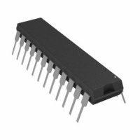
AD7712AN Analog Devices Inc, AD7712AN Datasheet - Page 5

AD7712AN
Manufacturer Part Number
AD7712AN
Description
IC ADC SIGNAL COND LC2MOS 24-DIP
Manufacturer
Analog Devices Inc
Datasheet
1.AD7712ARZ.pdf
(28 pages)
Specifications of AD7712AN
Data Interface
Serial
Rohs Status
RoHS non-compliant
Number Of Bits
24
Sampling Rate (per Second)
1.03k
Number Of Converters
1
Power Dissipation (max)
45mW
Voltage Supply Source
Analog and Digital, Dual ±
Operating Temperature
-40°C ~ 85°C
Mounting Type
Through Hole
Package / Case
24-DIP (0.300", 7.62mm)
Resolution (bits)
24bit
Sampling Rate
1.028kSPS
Input Channel Type
Differential
Supply Voltage Range - Digital
4.75V To 5.25V
Supply Current
4.5mA
Lead Free Status / RoHS Status
Contains lead / RoHS non-compliant
Available stocks
Company
Part Number
Manufacturer
Quantity
Price
Part Number:
AD7712AN
Manufacturer:
ADI/亚德诺
Quantity:
20 000
Company:
Part Number:
AD7712ANZ
Manufacturer:
ALTERA
Quantity:
300
TIMING CHARACTERISTICS
Parameter
f
t
t
t
t
t
Self-Clocking Mode
NOTES
1
2
3
4
5
6
7
REV. F
Guaranteed by design, not production tested. Sample tested during initial release and after any redesign or process change that may affect this parameter. All input
See Figures 11 to 14.
The AD7712 is specified with a 10 MHz clock for AV
CLK IN duty cycle range is 45% to 55%. CLK IN must be supplied whenever the AD7712 is not in STANDBY mode. If no clock is present in this case, the
The AD7712 is production tested with f
Specified using 10% and 90% points on waveform of interest.
These numbers are measured with the load circuit of Figure 1 and defined as the time required for the output to cross 0.8 V or 2.4 V.
CLK IN
CLK IN LO
CLK IN HI
r
f
1
signals are specified with tr = tf = 5 ns (10% to 90% of 5 V) and timed from a voltage level of 1.6 V.
than 10.5 V.
device can draw higher current than specified and possibly become uncalibrated.
6
6
t
t
t
t
t
t
t
t
t
t
t
t
t
t
t
2
3
4
5
6
7
8
9
10
14
15
16
17
18
19
7
7
4, 5
(A, S Versions)
Limit at T
400
10
8
0.4
0.4
50
50
1000
0
0
2
0
4
4
t
t
t
3
50
0
4
4
0
10
CLK IN
CLK IN
CLK IN
t
t
t
t
t
t
CLK IN
CLK IN
CLK IN
CLK IN
CLK IN
CLK IN
CLK IN
t
t
/2
/2 + 30
/2
CLK IN
CLK IN
at 10 MHz (8 MHz for AV
/2
MIN
+ 20
+ 20
+ 20
1, 2
, T
DD
MAX
voltages of 5 V ± 5%. It is specified with an 8 MHz clock for AV
(DV
0 V; f
DD
CLKIN
= +5 V
=10 MHz; Input Logic 0 = 0 V, Logic 1 = DV
Unit
kHz min
MHz max
MHz
ns min
ns min
ns max
ns max
ns min
ns min
ns min
ns min
ns min
ns max
ns max
ns min
ns max
ns nom
ns nom
ns min
ns min
ns max
ns min
ns min
ns min
DD
5%; AV
< 5.25 V). It is guaranteed by characterization to operate at 400 kHz.
–5–
DD
= +5 V or +10 V
Conditions/Comments
Master Clock Frequency: Crystal Oscillator or
Externally Supplied
AV
For Specified Performance
AV
Master Clock Input Low Time; t
Master Clock Input High Time
Digital Output Rise Time; Typically 20 ns
Digital Output Fall Time; Typically 20 ns
SYNC Pulse Width
DRDY to RFS Setup Time; t
DRDY to RFS Hold Time
A0 to RFS Setup Time
A0 to RFS Hold Time
RFS Low to SCLK Falling Edge
Data Access Time (RFS Low to Data Valid)
SCLK Falling Edge to Data Valid Delay
SCLK High Pulse Width
SCLK Low Pulse Width
A0 to TFS Setup Time
A0 to TFS Hold Time
TFS to SCLK Falling Edge Delay Time
TFS to SCLK Falling Edge Hold Time
Data Valid to SCLK Setup Time
Data Valid to SCLK Hold Time
DD
DD
= 5 V ± 5%
= 5.25 V to 10.5 V
3
5%; V
SS
DD
, unless otherwise noted.)
= 0 V or –5 V
DD
voltages greater than 5.25 V and less
CLK IN
CLK IN
= 1/f
= 1/f
5%; AGND = DGND =
CLK IN
CLK IN
AD7712


