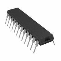
AD7712AN Analog Devices Inc, AD7712AN Datasheet - Page 24

AD7712AN
Manufacturer Part Number
AD7712AN
Description
IC ADC SIGNAL COND LC2MOS 24-DIP
Manufacturer
Analog Devices Inc
Datasheet
1.AD7712ARZ.pdf
(28 pages)
Specifications of AD7712AN
Data Interface
Serial
Rohs Status
RoHS non-compliant
Number Of Bits
24
Sampling Rate (per Second)
1.03k
Number Of Converters
1
Power Dissipation (max)
45mW
Voltage Supply Source
Analog and Digital, Dual ±
Operating Temperature
-40°C ~ 85°C
Mounting Type
Through Hole
Package / Case
24-DIP (0.300", 7.62mm)
Resolution (bits)
24bit
Sampling Rate
1.028kSPS
Input Channel Type
Differential
Supply Voltage Range - Digital
4.75V To 5.25V
Supply Current
4.5mA
Lead Free Status / RoHS Status
Contains lead / RoHS non-compliant
Available stocks
Company
Part Number
Manufacturer
Quantity
Price
Part Number:
AD7712AN
Manufacturer:
ADI/亚德诺
Quantity:
20 000
Company:
Part Number:
AD7712ANZ
Manufacturer:
ALTERA
Quantity:
300
AD7712
SIMPLIFYING THE EXTERNAL CLOCKING MODE
INTERFACE
In many applications, the user may not require the facility of
writing to the on-chip calibration registers. In this case, the
serial interface to the AD7712 in external clocking mode can be
simplified by connecting the TFS line to the A0 input of the
AD7712 (see Figure 15). This means that any write to the device
will load data to the control register (since A0 is low while TFS
is low), and any read to the device will access data from the out-
put data register or from the calibration registers (since A0 is
high while RFS is low). It should be noted that in this arrange-
ment the user does not have the capability of reading from the
control register.
Another method of simplifying the interface is to generate the
TFS signal from an inverted RFS signal. However, generating
the signals the opposite way around (RFS from an inverted
TFS) will cause writing errors.
MICROCOMPUTER/MICROPROCESSOR INTERFACING
The AD7712’s flexible serial interface allows easy interface to
most microcomputers and microprocessors. Figure 16 shows a
flowchart diagram for a typical programming sequence for read-
ing data from the AD7712 to a microcomputer while Figure 17
shows a flowchart diagram for writing data to the AD7712.
Figures 18, 19, and 20 show some typical interface circuits.
The flowchart of Figure 16 is for continuous read operations
from the AD7712 output register. In the example shown, the
DRDY line is continuously polled. Depending on the micro-
processor configuration, the DRDY line may come to an
interrupt input, in which case the DRDY will automatically
generate an interrupt without being polled. Reading the serial
buffer could be anything from one read operation up to three
read operations (where 24 bits of data are read into an 8-bit
serial register). A read operation to the control/calibration
registers is similar, but, in this case, the status of DRDY can
be ignored. The A0 line is brought low when the RFS line is
brought low when reading from the control register.
The flowchart also shows the bits being reversed after they have
been read in from the serial port. This depends on whether the
microprocessor expects the MSB of the word first or the LSB of
the word first. The AD7712 outputs the MSB first.
Figure 15. Simplified Interface with TFS Connected to A0
FOUR INTER-
FACE LINES
SDATA
RFS
SCLK
TFS
A0
AD7712
–24–
The flowchart in Figure 17 is for a single 24-bit write operation
to the AD7712 control or calibration registers. This shows data
being transferred from data memory to the accumulator before
being written to the serial buffer. Some microprocessor systems
will allow data to be written directly to the serial buffer from data
memory. Writing data to the serial buffer from the accumulator
will generally consist of either two or three write operations,
depending on the size of the serial buffer.
The flowchart also shows the option of the bits being reversed
before being written to the serial buffer. This depends on
whether the first bit transmitted by the microprocessor is the
MSB or the LSB. The AD7712 expects the MSB as the first bit
in the data stream. In cases where the data is being read or
being written in bytes and the data has to be reversed, the bits
will have to be reversed for every byte.
Figure 16. Flowchart for Continuous Read
Operations to the AD7712
CONFIGURE AND
INITIALIZE C/ P
SERIAL BUFFER
ORDER OF BITS
RFS, TFS HIGH
SERIAL PORT
POLL DRDY
RFS LOW
RFS HIGH
REVERSE
START
BRING
BRING
LOW?
BRING
DRDY
READ
YES
NO
3
REV. F


