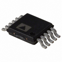
AD7686BRMZ Analog Devices Inc, AD7686BRMZ Datasheet - Page 13

AD7686BRMZ
Manufacturer Part Number
AD7686BRMZ
Description
IC ADC 16BIT 500KSPS 10-MSOP
Manufacturer
Analog Devices Inc
Series
PulSAR®r
Specifications of AD7686BRMZ
Data Interface
DSP, MICROWIRE™, QSPI™, Serial, SPI™
Number Of Bits
16
Sampling Rate (per Second)
500k
Number Of Converters
1
Power Dissipation (max)
21.5mW
Voltage Supply Source
Single Supply
Operating Temperature
-40°C ~ 85°C
Mounting Type
Surface Mount
Package / Case
10-TFSOP (0.118", 3.00mm Width)
Resolution (bits)
16bit
Input Channel Type
Pseudo Differential
Supply Voltage Range - Analogue
4.5V To 5.5V
Supply Voltage Range - Digital
1.8V To 5.8V, 2.3V To 5.8V
Sampling Rate
500kSPS
Rohs Compliant
Yes
Lead Free Status / RoHS Status
Lead free / RoHS Compliant
For Use With
EVAL-AD7686CBZ - BOARD EVALUATION FOR AD7686
Lead Free Status / RoHS Status
Lead free / RoHS Compliant, Lead free / RoHS Compliant
Available stocks
Company
Part Number
Manufacturer
Quantity
Price
Company:
Part Number:
AD7686BRMZ
Manufacturer:
ADI
Quantity:
1 000
Part Number:
AD7686BRMZ
Manufacturer:
ADI/亚德诺
Quantity:
20 000
Part Number:
AD7686BRMZ-REEL
Manufacturer:
ADI/亚德诺
Quantity:
20 000
Part Number:
AD7686BRMZ-RL7
Manufacturer:
ADI/亚德诺
Quantity:
20 000
Company:
Part Number:
AD7686BRMZRL7
Manufacturer:
ADI
Quantity:
1 000
Part Number:
AD7686BRMZRL7
Manufacturer:
ADI/亚德诺
Quantity:
20 000
Transfer Functions
The ideal transfer characteristic for the AD7686 is shown in
Figure 25 and Table 7.
000...010
000...001
000...000
111...110
111...101
111...111
–FSR + 0.5 LSB
–FSR
Figure 25. ADC Ideal Transfer Function
–FSR + 1 LSB
0 TO VREF
ANALOG INPUT
1
2
3
4
5
SEE THE VOLTAGE REFERENCE INPUT SECTION FOR REFERENCE SELECTION.
C
SEE DRIVER AMPLIFIER CHOICE SECTION.
OPTIONAL FILTER. SEE ANALOG INPUT SECTION.
SEE DIGITAL INTERFACE SECTION FOR MOST CONVENIENT INTERFACE MODE.
3
REF
≤–2V
≥7V
≥7V
+FSR – 1.5 LSB
IS USUALLY A 10µF CERAMIC CAPACITOR (X5R).
Figure 26. Typical Application Diagram with Multiple Supplies
REF
4
2.7nF
+FSR – 1 LSB
33Ω
1
10µF
2
IN+
IN–
Rev. B | Page 13 of 28
GND
REF
AD7686
VDD
Table 7. Output Codes and Ideal Input Voltages
Description
FSR – 1 LSB
Midscale + 1 LSB
Midscale
Midscale – 1 LSB
–FSR + 1 LSB
–FSR
TYPICAL CONNECTION DIAGRAM
Figure 26 shows an example of the recommended connection
diagram for the AD7686 when multiple supplies are available.
1
2
This is also the code for an overranged analog input (V
This is also the code for an underranged analog input (V
VIO
SCK
SDO
CNV
SDI
100nF
100nF
3- OR 4-WIRE INTERFACE
Analog Input
V
4.999924 V
2.500076 V
2.5 V
2.499924 V
76.3 μV
0 V
5V
1.8V TO VDD
REF
= 5 V
Digital Output Code
Hexadecimal
FFFF
8001
8000
7FFF
0001
0000
5
1
2
IN+
− V
IN+
IN−
− V
above V
AD7686
IN−
below V
REF
− V
GND
GND
).
).


