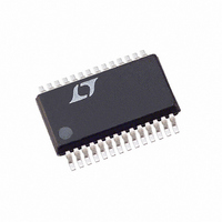
LTC2408CG#TR Linear Technology, LTC2408CG#TR Datasheet - Page 22

LTC2408CG#TR
Manufacturer Part Number
LTC2408CG#TR
Description
IC ADC 24BIT 8CH MICROPWR 28SSOP
Manufacturer
Linear Technology
Datasheet
1.LTC2408CGPBF.pdf
(36 pages)
Specifications of LTC2408CG#TR
Number Of Bits
24
Sampling Rate (per Second)
7.5
Data Interface
MICROWIRE™, Serial, SPI™
Number Of Converters
1
Power Dissipation (max)
1mW
Voltage Supply Source
Single Supply
Operating Temperature
0°C ~ 70°C
Mounting Type
Surface Mount
Package / Case
28-SSOP (0.200", 5.30mm Width)
Lead Free Status / RoHS Status
Contains lead / RoHS non-compliant
Available stocks
Company
Part Number
Manufacturer
Quantity
Price
APPLICATIONS
LTC2404/LTC2408
mode. However, certain applications may require an exter-
nal driver on SCK. If this driver goes Hi-Z after outputting
a LOW signal, the LTC2404/LTC2408’s internal pull-up
remains disabled. Hence, SCK remains LOW. On the next
falling edge of CSADC, the device is switched to the
external SCK timing mode. By adding an external 10k pull-
up resistor to SCK, this pin goes HIGH once the external
driver goes Hi-Z. On the next CSADC falling edge, the
device will remain in the internal SCK timing mode.
A similar situation may occur during the sleep state when
CSADC is pulsed HIGH-LOW-HIGH in order to test the
conversion status. If the device is in the sleep state
(EOC = 0), SCK will go LOW. Once CSADC goes HIGH
(within the time period defined above as t
internal pull-up is activated. For a heavy capacitive load
on the SCK pin, the internal pull-up may not be adequate
to return SCK to a HIGH level before CSADC goes LOW
again. This is not a concern under normal conditions
where CSADC remains LOW after detecting EOC = 0. This
situation is easily avoided by adding an external 10k pull-
up resistor to the SCK pin.
DIGITAL SIGNAL LEVELS
The LTC2404/LTC2408’s digital interface is easy to use.
Its digital inputs (F
in External SCK mode of operation) accept standard TTL/
CMOS logic levels and can tolerate edge rates as slow as
100 s. However, some considerations are required to take
advantage of exceptional accuracy and low supply current.
The digital output signals (SDO and SCK in Internal SCK
mode of operation) are less of a concern because they are
not generally active during the conversion state.
In order to preserve the accuracy of the LTC2404/LTC2408,
it is very important to minimize the ground path imped-
ance which may appear in series with the input and/or
reference signal and to reduce the current which may flow
through this path. Pin 6 (GND) should be connected to a
low resistance ground plane through a minimum length
trace. The use of multiple via holes is recommended to
further reduce the connection resistance. The LTC2404/
LTC2408’s power supply current flowing through the
0.01 resistance of the common ground pin will develop
22
O
U
, CSADC, CSMUX, CLK, D
INFORMATION
U
W
EOCtest
IN
U
and SCK
), the
a 2.5 V offset signal. For a reference voltage V
this represents a 1ppm offset error.
In an alternative configuration, Pin 6 (GND) of the converter
can be the single-point-ground in a single point grounding
system. The input signal ground, the reference signal
ground, the digital drivers ground (usually the digital
ground) and the power supply ground (the analog ground)
should be connected in a star configuration with the com-
mon point located as close to Pin 6 as possible.
The power supply current during the conversion state
should be kept to a minimum. This is achieved by restrict-
ing the number of digital signal transitions occurring
during this period.
While a digital input signal is in the 0.5V to (V
range, the CMOS input receiver draws additional current
from the power supply. It should be noted that, when any
one of the digital input signals (F
CLK and SCK in External SCK mode of operation) is within
this range, the LTC2404/LTC2408 power supply current
may increase even if the signal in question is at a valid logic
level. For micropower operation and in order to minimize
the potential errors due to additional ground pin current,
it is recommended to drive all digital input signals to full
CMOS levels [V
Severe ground pin current disturbances can also occur
due to the undershoot of fast digital input signals. Under-
shoot and overshoot can occur because of the imped-
ance mismatch at the converter pin when the transition
time of an external control signal is less than twice the
propagation delay from the driver to LTC2404/LTC2408.
For reference, on a regular FR-4 board, signal propaga-
tion velocity is approximately 183ps/inch for internal
traces and 170ps/inch for surface traces. Thus, a driver
generating a control signal with a minimum transition
time of 1ns must be connected to the converter pin
through a trace shorter than 2.5 inches. This problem
becomes particularly difficult when shared control lines
are used and multiple reflections may occur. The solution
is to carefully terminate all transmission lines close to
their characteristic impedance.
Parallel termination near the LTC2404/LTC2408 input
pins will eliminate this problem but will increase the driver
IL
< 0.4V and V
OH
O
, CSADC, CSMUX, D
> (V
CC
– 0.4V)].
REF
CC
– 0.5V)
= 2.5V,
IN
,


