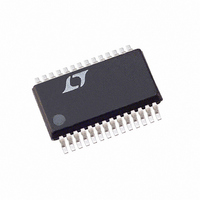
LTC2408CG#TR Linear Technology, LTC2408CG#TR Datasheet - Page 10

LTC2408CG#TR
Manufacturer Part Number
LTC2408CG#TR
Description
IC ADC 24BIT 8CH MICROPWR 28SSOP
Manufacturer
Linear Technology
Datasheet
1.LTC2408CGPBF.pdf
(36 pages)
Specifications of LTC2408CG#TR
Number Of Bits
24
Sampling Rate (per Second)
7.5
Data Interface
MICROWIRE™, Serial, SPI™
Number Of Converters
1
Power Dissipation (max)
1mW
Voltage Supply Source
Single Supply
Operating Temperature
0°C ~ 70°C
Mounting Type
Surface Mount
Package / Case
28-SSOP (0.200", 5.30mm Width)
Lead Free Status / RoHS Status
Contains lead / RoHS non-compliant
Available stocks
Company
Part Number
Manufacturer
Quantity
Price
FU CTIO AL BLOCK DIAGRA
V
LTC2404/LTC2408
PIN
state aborts the data transfer and starts a new conversion.
For normal operation, drive this pin in parallel with CSMUX.
SDO (Pin 24): Three-State Digital Output. During the data
output period this pin is used for serial data output. When
the chip select CSADC is high (CSADC = V
is in a high impedance state. During the Conversion and
Sleep periods, this pin can be used as a conversion status
output. The conversion status can be observed by pulling
CSADC low.
SCK (Pin 25): Shift Clock for Data Out. This clock synchro-
nizes the serial data transfer of the ADC data output. Data
is shifted out of SDO on the falling edge of SCK. For normal
operation, drive this pin in parallel with CLK.
TEST CIRCUITS
GND
10
CH0
CH1
CH2
CH3
CH4
CH5
CH6
CH7
V
REF
CC
U
U
FUNCTIONS
U
U
SDO
U
Hi-Z TO V
V
V
3.4k
OL
OH
DAC
TO V
TO Hi-Z
OH
OH
C
LOAD
CC
24048 TC01
), the SDO pin
= 20pF
W
F
frequencies and conversion time. When the F
connected to V
oscillator and the digital filter first null is located at 50Hz.
When the F
converter uses its internal oscillator and the digital filter
first null is located at 60Hz. When F
external clock signal with a frequency f
uses this signal as its clock and the digital filter first null is
located at a frequency f
word rate is f
O
(Pin 26): Digital input which controls the ADC’s notch
ADC
O
EOSC
CC
pin is connected to GND (F
SDO
(F
/20480.
O
Hi-Z TO V
V
V
AUTOCALIBRATION
DECIMATING FIR
OH
OL
= V
AND CONTROL
V
TO Hi-Z
TO V
CC
CC
EOSC
3.4k
C
OL
OL
), the converter uses its internal
LOAD
/2560. The resulting output
24048 TC02
= 20pF
OSCILLATOR
INTERFACE
INTERNAL
EOSC
CHANNEL
O
SERIAL
SELECT
is driven by an
, the converter
O
= OV), the
24048 BD
(INT/EXT)
O
pin is
F
SDO
SCK
CSADC
CSMUX
D
CLK
O
IN


