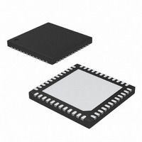
MAX19516ETM+ Maxim Integrated Products, MAX19516ETM+ Datasheet - Page 32

MAX19516ETM+
Manufacturer Part Number
MAX19516ETM+
Description
IC ADC 10BIT 100MSPS DUAL 48TQFN
Manufacturer
Maxim Integrated Products
Datasheet
1.MAX19516ETM.pdf
(35 pages)
Specifications of MAX19516ETM+
Number Of Bits
10
Sampling Rate (per Second)
100M
Data Interface
Serial, Parallel
Number Of Converters
2
Voltage Supply Source
Analog and Digital
Operating Temperature
-40°C ~ 85°C
Mounting Type
Surface Mount
Package / Case
48-TQFN Exposed Pad
Conversion Rate
100 MSPs
Resolution
10 bit
Interface Type
SPI
Snr
60.1 dB
Voltage Reference
1.25 V
Supply Voltage (max)
3.5 V
Supply Voltage (min)
1.7 V
Maximum Power Dissipation
3200 mW
Maximum Operating Temperature
+ 85 C
Mounting Style
SMD/SMT
Input Voltage
1.8 V
Minimum Operating Temperature
- 40 C
Lead Free Status / RoHS Status
Lead free / RoHS Compliant
Dual-Channel, 10-Bit, 100Msps ADC
Figure 20. Single-Ended, AC-Coupled Input Drive
The circuit of Figure 19 also converts a single-ended
input signal to a fully differential signal. Figure 19 uti-
lizes an additional transformer to improve the common-
mode rejection allowing high-frequency signals beyond
the Nyquist frequency. A set of 75Ω and 110Ω termina-
tion resistors provide an equivalent 50Ω termination to
the signal source. The second set of termination resis-
tors connect to CM_ providing the correct input com-
mon-mode voltage.
Figure 20 shows a single-ended, AC-coupled input
application. The MAX4108 provides high speed, high
bandwidth, low noise, and low distortion to maintain the
input signal integrity. Bias voltage is applied to the
inputs through internal 2kΩ resistors. See Common
Mode register 08h for further details.
The MAX19516’s wide common-mode voltage range
(0.4V to 1.4V) allows DC-coupled signals. Ensure that the
common-mode voltage remains between 0.4V and 1.4V.
Figure 21 shows a single-ended-to-differential clock
input converting circuit.
The MAX19516 requires high-speed board-layout
design techniques. Locate all bypass capacitors as
close as possible to the device, preferably on the same
side as the ADC, using surface-mount devices for mini-
mum inductance. Bypass AVDD, OVDD, REFIO, CMA,
and CMB with 0.1µF ceramic capacitors to GND.
Multilayer boards with ground and power planes
32
V
______________________________________________________________________________________
IN
Board-Layout Considerations
MAX4108
Grounding, Bypassing, and
Single-Ended AC-Coupled Input Signal
100Ω
100Ω
0.1µF
0.1µF
0.1µF
IN_+
CM_
IN_-
DC-Coupled Input
MAX19516
Clock Input
Figure 21. Single-Ended-to-Differential Clock Input
produce the highest level of signal integrity. Route high-
speed digital signal traces away from the sensitive ana-
log traces of either channel. Make sure to isolate the
analog input lines to each respective converter to mini-
mize channel-to-channel crosstalk. Keep all signal lines
short and free of 90° turns.
INL is the deviation of the measured transfer function
from a best-fit straight line. Worst-case deviation is
defined as INL.
DNL is the difference between the measured transfer
function step width and the ideal value of 1 LSB. A DNL
error specification of less than 1 LSB guarantees no
missing codes and a monotonic transfer function. DNL
deviations are measured at each step of the transfer
function and the worst-case deviation is defined as DNL.
Offset error is a parameter that indicates how well the
actual transfer function matches the ideal transfer func-
tion at midscale. Ideally, the midscale transition occurs
at 0.5 LSB above midscale. The offset error is the
amount of deviation between the measured midscale
transition point and the ideal midscale transition point.
Gain error is a figure of merit that indicates how well the
slope of the measured transfer function matches the
slope of the ideal transfer function based on the speci-
fied full-scale input-voltage range. The gain error is
defined as the relative error of the measured transfer
function and is expressed as a percentage.
CLKIN
0.1µF
Differential Nonlinearity (DNL)
49.9Ω
49.9Ω
Integral Nonlinearity (INL)
0.01µF
0.01µF
Definitions
CLK+
CLK-
Offset Error
MAX19516
Gain Error


