MAX19516ETM+ Maxim Integrated Products, MAX19516ETM+ Datasheet - Page 25

MAX19516ETM+
Manufacturer Part Number
MAX19516ETM+
Description
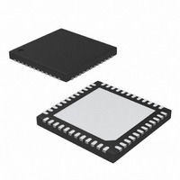
IC ADC 10BIT 100MSPS DUAL 48TQFN
Manufacturer
Maxim Integrated Products
Datasheet
1.MAX19516ETM.pdf
(35 pages)
Specifications of MAX19516ETM+
Number Of Bits
10
Sampling Rate (per Second)
100M
Data Interface
Serial, Parallel
Number Of Converters
2
Voltage Supply Source
Analog and Digital
Operating Temperature
-40°C ~ 85°C
Mounting Type
Surface Mount
Package / Case
48-TQFN Exposed Pad
Conversion Rate
100 MSPs
Resolution
10 bit
Interface Type
SPI
Snr
60.1 dB
Voltage Reference
1.25 V
Supply Voltage (max)
3.5 V
Supply Voltage (min)
1.7 V
Maximum Power Dissipation
3200 mW
Maximum Operating Temperature
+ 85 C
Mounting Style
SMD/SMT
Input Voltage
1.8 V
Minimum Operating Temperature
- 40 C
Lead Free Status / RoHS Status
Lead free / RoHS Compliant
Figure 10. Multiplexed Output Mode Timing
Format/Test Pattern register (06h) for clock-divider
options, or in parallel programming configuration (SPEN
= 1) by using the DIV input.
Figures 9 and 10 depict the relationship between the
clock input and output, analog input, sampling event,
and data output. The MAX19516 samples on the rising
edge of the sampling clock. Output data is valid on the
next rising edge of DCLK after a nine-clock internal
latency. For applications where the clock is divided, the
sample clock is the divided internal clock derived from:
When using the clock divider, the phase of the internal
clock can be different than that of the FPGA, microcon-
troller, or other MAX19516s in the system. There are
SAMPLE CLOCK
DATA, DOR
SAMPLE CLOCK IS THE DERIVED CLOCK FROM (CLK+ - CLK-)/CLOCK DIVIDER, IN_ = IN_+ - IN_-.
MUX_CH (BIT 2, OUTPUT FORMAT 01h) DETERMINES THE OUTPUT BUS AND WHICH CHANNEL DATA IS PRESENTED.
DCLK
IN_
[(CLK+ - CLK-)/DIVIDER]
System Timing Requirements
______________________________________________________________________________________
t
DD
SAMPLING
INSTANT
CHB
n-10
Dual-Channel, 10-Bit, 100Msps ADC
SAMPLE ON RISING EDGE
n
t
AD
CHA
n-9
t
DC
Synchronization
SAMPLING
INSTANT
CHB
n-9
n+1
t
DCH
CHA
t
n-8
CHA
SAMPLING
t
INSTANT
DCL
CHB
n-8
n+2
t
CH
t
CHA
CLK
n-7
two mechanisms to synchronize the internal clock: slip
synchronization and edge synchronization. Select the
synchronization mode using SYNC_MODE (bit 2) in the
Clock Divide/Data Format/Test Pattern register (06h)
and drive the SYNC input high to synchronize.
Slip Synchronization Mode, SYNC_MODE = 0
(default): On the third rising edge of the input clock
(CLK) after the rising edge of SYNC (provided set-up
and hold times are met), the divided output is forced to
skip a state transition (Figure 11).
Edge Synchronization Mode, SYNC_MODE = 1: On
the third rising edge of the input clock (CLK) after the
rising edge of SYNC (provided set-up and hold times
are met), the divided output is forced to state 0. A divid-
ed clock rising edge occurs on the fourth (/2 mode) or
fifth (/4 mode) rising edge of CLK, after a valid rising
edge of SYNC (Figure 12).
MUX OUTPUT MODE
SAMPLING
INSTANT
t
SETUP
CHB
t
n-7
CHB
n+3
CHA
n-6
t
HOLD
t
CL
SAMPLING
INSTANT
CHB
n-6
n+4
t
SETUP
CHA
n-5
SAMPLING
INSTANT
CHB
n-5
t
HOLD
n+5
CHA
n-4
CHB
n-4
25


