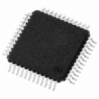
TSA1204IFT STMicroelectronics, TSA1204IFT Datasheet - Page 19

TSA1204IFT
Manufacturer Part Number
TSA1204IFT
Description
IC CONV A/D 2-CH 12-BIT 48-TQFP
Manufacturer
STMicroelectronics
Datasheet
1.TSA1204IFT.pdf
(31 pages)
Specifications of TSA1204IFT
Number Of Bits
12
Sampling Rate (per Second)
20M
Data Interface
Parallel
Number Of Converters
2
Power Dissipation (max)
155mW
Voltage Supply Source
Analog and Digital
Operating Temperature
-40°C ~ 85°C
Mounting Type
Surface Mount
Package / Case
48-TQFP
Lead Free Status / RoHS Status
Lead free / RoHS Compliant
Other names
497-5435-2
TSA1204IFT
TSA1204IFT
Available stocks
Company
Part Number
Manufacturer
Quantity
Price
Company:
Part Number:
TSA1204IFT
Manufacturer:
PHI
Quantity:
45
Company:
Part Number:
TSA1204IFT
Manufacturer:
STMicroelectronics
Quantity:
10 000
TSA1204
8.6
8.7
Table 12.
Layout precautions
To use the ADC circuits most efficiently at high frequencies, some precautions have to be
taken for power supplies:
●
●
●
●
●
EVAL1204/BA evaluation board
The EVAL1204/BA is a 4-layer board with high decoupling and grounding level. The
schematic of the evaluation board is shown in
Figure
in
Figure 28. Analog-to-digital converter characterization bench
F
R
Optimized power (mW)
S
pol
Figure
(Msps)
First of all, the implementation of 4 proper separate supplies and ground planes
(analog, digital, internal and external buffer ones) on the PCB is recommended for high
speed circuit applications to provide low inductance and low resistance common return.
The separation of the analog signal from the digital output part is mandatory to prevent
noise from coupling onto the input signal. The best compromise is to connect AGND,
DGND, GNDBI in a common point whereas GNDBE must be isolated. Similarly, the
AVCC, DVCC and VCCBI power supplies must be separate from the VCCBE power
supply.
Power supply bypass capacitors must be placed as close as possible to the IC pins in
order to improve high frequency bypassing and reduce harmonic distortion.
All inputs and outputs must be properly terminated with output termination resistors;
then the amplifier load is resistive only and the stability of the amplifier is improved. All
leads must be wide and as short as possible especially for the analog input in order to
decrease parasitic capacitance and inductance.
To keep the capacitive loading as low as possible at digital outputs, short lead lengths
of routing are essential to minimize currents when the output changes. To minimize this
output capacitance, use buffers or latches close to the output pins.
Choose component sizes as small as possible (SMD).
(
kΩ)
29. The board has been characterized with a fully devoted ADC test bench as shown
28.
Sine Wave
Generator
HP8644
Total power consumption optimization depending on R
HP8133
HP8644
Vin
Sine Wave
Generator
evaluation
Generator
board
Pulse
ADC
120
10
95
Figure 30
Clk
Data
Clk
and its top overlay view in
Analyzer
Logic
Application information
pol
120
20
54
value
PC
19/31


