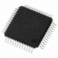
TSA1204IFT STMicroelectronics, TSA1204IFT Datasheet - Page 15

TSA1204IFT
Manufacturer Part Number
TSA1204IFT
Description
IC CONV A/D 2-CH 12-BIT 48-TQFP
Manufacturer
STMicroelectronics
Datasheet
1.TSA1204IFT.pdf
(31 pages)
Specifications of TSA1204IFT
Number Of Bits
12
Sampling Rate (per Second)
20M
Data Interface
Parallel
Number Of Converters
2
Power Dissipation (max)
155mW
Voltage Supply Source
Analog and Digital
Operating Temperature
-40°C ~ 85°C
Mounting Type
Surface Mount
Package / Case
48-TQFP
Lead Free Status / RoHS Status
Lead free / RoHS Compliant
Other names
497-5435-2
TSA1204IFT
TSA1204IFT
Available stocks
Company
Part Number
Manufacturer
Quantity
Price
Company:
Part Number:
TSA1204IFT
Manufacturer:
PHI
Quantity:
45
Company:
Part Number:
TSA1204IFT
Manufacturer:
STMicroelectronics
Quantity:
10 000
TSA1204
8
8.1
8.1.1
8.1.2
Application information
The TSA1204 is a dual-channel, 12-bit resolution analog-to-digital converter based on a
pipeline structure and the latest deep submicron CMOS process to achieve the best
performance in terms of linearity and power consumption.
Each channel achieves 12-bit resolution through the pipeline structure which consists of 12
internal conversion stages in which the analog signal is fed and sequentially converted into
digital data. A latency time of 7 clock periods is necessary to obtain the digitized data on the
output bus.
The input signals are simultaneously sampled, for both channels, on the rising edge of the
clock. The output data is delivered on the rising edge of the clock for channel I and on the
falling edge of the clock for channel Q, as shown in
digital data produced at the different stages must be time delayed accordidng to the order of
conversion. Fianlly, a digital data correction completes the processing and ensures the
validity of the ending codes on the output bus.
The structure is specifically designed to accept differential signals only.
Additional functions
To simplify the application board as much as possible, the following operating modes are
provided:
●
●
Output enable mode (OEB)
When set to low level (V
When set to high level (V
converter goes on sampling. When OEB is set to a low level again, the data arrives on the
output with a very short T
Figure 2: Timing diagram on page 4
If you do not want to use OEB mode, the OEB pin should be grounded through a low value
resistor.
Select mode (SELECT)
The digital data output from each of the ADC cores is multiplexed to share the same output
bus. This prevents an increase in the number of pins and allows to use the same package as
for a single-channel ADC like the TSA1201.
The information channel is selected with the "SELECT" pin. When set to high level (V
channel I data is present on the D0-D11 output bus. When set to low level (V
data is delivered on D0-D11.
By connecting SELECT to CLK, channel I and channel Q are simultaneously present on D0-
D11, channel I on the rising edge of the clock and channel Q on the falling edge of the clock.
(Refer to
Output enable mode (OEB)
Select mode (SELECT)
Figure 2: Timing diagram on page
IL
IH
on
), all digital outputs remain active and are in low impedance state.
), all digital output buffers are in high impedance state while the
delay. This mechanism allows the chip select of the device.
summarizes this functionality.
4).
Figure 2: Timing diagram on page
Application information
IL
), channel Q
4. The
IH
15/31
),


