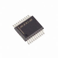
MAX1202BEAP+ Maxim Integrated Products, MAX1202BEAP+ Datasheet - Page 8

MAX1202BEAP+
Manufacturer Part Number
MAX1202BEAP+
Description
IC ADC 12BIT 8CH 20-SSOP
Manufacturer
Maxim Integrated Products
Datasheet
1.MAX1202BCPP.pdf
(24 pages)
Specifications of MAX1202BEAP+
Number Of Bits
12
Sampling Rate (per Second)
133k
Data Interface
MICROWIRE™, Serial, SPI™
Number Of Converters
1
Power Dissipation (max)
640mW
Voltage Supply Source
Dual ±
Operating Temperature
-40°C ~ 85°C
Mounting Type
Surface Mount
Package / Case
20-SSOP
Number Of Adc Inputs
8
Architecture
SAR
Conversion Rate
133 KSPs
Resolution
12 bit
Input Type
Voltage
Interface Type
Serial
Voltage Reference
Internal 4.096 V or External
Supply Voltage (max)
5 V
Maximum Power Dissipation
640 mW
Maximum Operating Temperature
+ 85 C
Mounting Style
SMD/SMT
Input Voltage
4.096 V
Minimum Operating Temperature
- 40 C
Lead Free Status / RoHS Status
Lead free / RoHS Compliant
5V, 8-Channel, Serial, 12-Bit ADCs
with 3V Digital Interface
(V
(133ksps); MAX1202—4.7µF capacitor at REF pin; MAX1203—external reference, V
unless otherwise noted.)
8
______________________________________________________________Pin Description
____________________________Typical Operating Characteristics (continued)
DD
PIN
1–8
10
11
12
13
14
15
16
17
18
19
20
_______________________________________________________________________________________
9
= 5V ±5%; VL = 2.7V to 3.6V; V
CH0–CH7
REFADJ
SSTRB
NAME
SHDN
DOUT
SCLK
GND
REF
V
V
DIN
CS
VL
DD
SS
-0.2
-0.4
-0.6
-0.8
-1.0
1.0
0.8
0.6
0.4
0.2
0
0
750
Sampling Analog Inputs
Negative Supply Voltage. Tie V
Three-Level Shutdown Input. Pulling SHDN low shuts the MAX1202/MAX1203 down to 10µA (max)
supply current; otherwise, the MAX1202/MAX1203 are fully operational. Pulling SHDN to V
reference-buffer amplifier in internal compensation mode. Letting SHDN float puts the reference-
buffer amplifier in external compensation mode.
Reference-Buffer Output/ADC Reference Input. In internal reference mode (MAX1202 only), the refer-
ence buffer provides a 4.096V nominal output, externally adjustable at REFADJ. In external reference
mode, disable the internal buffer by pulling REFADJ to V
Input to the Reference-Buffer Amplifier. Tie REFADJ to V
Ground; IN- Input for Single-Ended Conversions
Supply Voltage for Digital Output Pins. Voltage applied to VL determines the positive output swing of
the Digital Outputs (DOUT, SSTRB). 2.7V ≤ VL ≤ 5.25V.
Serial-Data Output. Data is clocked out at SCLK’s falling edge. High impedance when CS is high.
Serial-Strobe Output. In internal clock mode, SSTRB goes low when the MAX1202/MAX1203 begin
the analog-to-digital conversion, and goes high when the conversion is finished. In external clock
mode, SSTRB pulses high for one clock period before the MSB decision. High impedance when CS
is high (external clock mode).
Serial-Data Input. Data is clocked in at SCLK’s rising edge.
Active-Low Chip Select. Data is not clocked into DIN unless CS is low. When CS is high, DOUT is
high impedance.
Serial-Clock Input. SCLK clocks data in and out of the serial interface. In external clock mode, SCLK
also sets the conversion speed. (Duty cycle must be 40% to 60% in external clock mode.)
Positive Supply Voltage, +5V ±5%
INTEGRAL NONLINEARITY
1500
vs. DIGITAL
DIGITAL CODE
2250
SS
= 0V; f
3000
SCLK
3750
= 2.0MHz, external clock (50% duty cycle); 15 clocks/conversion cycle
4500
SS
to -5V ±5% or to GND.
-100
-120
-20
-40
-60
-80
FUNCTION
20
0
0
REF
DD
DD.
= 4.096V applied to REF pin; T
FREQUENCY (kHz)
to disable the reference-buffer amplifier.
FFT PLOT
33.25
V
SS
= -5V
66.50
DD
A
= +25°C;
puts the


