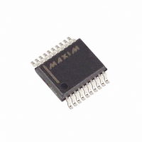
MAX1202BEAP+ Maxim Integrated Products, MAX1202BEAP+ Datasheet - Page 22

MAX1202BEAP+
Manufacturer Part Number
MAX1202BEAP+
Description
IC ADC 12BIT 8CH 20-SSOP
Manufacturer
Maxim Integrated Products
Datasheet
1.MAX1202BCPP.pdf
(24 pages)
Specifications of MAX1202BEAP+
Number Of Bits
12
Sampling Rate (per Second)
133k
Data Interface
MICROWIRE™, Serial, SPI™
Number Of Converters
1
Power Dissipation (max)
640mW
Voltage Supply Source
Dual ±
Operating Temperature
-40°C ~ 85°C
Mounting Type
Surface Mount
Package / Case
20-SSOP
Number Of Adc Inputs
8
Architecture
SAR
Conversion Rate
133 KSPs
Resolution
12 bit
Input Type
Voltage
Interface Type
Serial
Voltage Reference
Internal 4.096 V or External
Supply Voltage (max)
5 V
Maximum Power Dissipation
640 mW
Maximum Operating Temperature
+ 85 C
Mounting Style
SMD/SMT
Input Voltage
4.096 V
Minimum Operating Temperature
- 40 C
Lead Free Status / RoHS Status
Lead free / RoHS Compliant
Figure 19 shows an application circuit to interface the
MAX1202/MAX1203 to the TMS320 in external clock mode.
Figure 20 shows the timing diagram for this interface circuit.
Use the following steps to initiate a conversion in the
MAX1202/MAX1203 and to read the results:
1) The TMS320 should be configured with CLKX (trans-
2) The MAX1202/MAX1203’s CS is driven low by the
5V, 8-Channel, Serial, 12-Bit ADCs
with 3V Digital Interface
Figure 18. Power-Supply Grounding Connection
Figure 20. TMS320 Serial-Interface Timing Diagram
22
mit clock) as an active-high output clock and CLKR
(TMS320 receive clock) as an active-high input clock.
The TMS320’s CLKX and CLKR are tied together with
the MAX1202/MAX1203’s SCLK input.
TMS320’s XF_ I/O port to enable data to be clocked
into the MAX1202/MAX1203’s DIN.
SSTRB
DOUT
SCLK
______________________________________________________________________________________
*OPTIONAL
DIN
CS
V
+5V
DD
R* = 10
START
MAX1202
MAX1203
GND
SEL2
TMS320CL3x to MAX1202/
SUPPLIES
V
-5V
SS
SEL1
MAX1203 Interface
VL
SEL0
+3V
+3V
UNI/BIP SGL/DIF
CIRCUITRY
DIGITAL
DGND
GND
PD1
PD0
3) Write an 8-bit word (1XXXXX11) to the MAX1202/
4) The MAX1202/MAX1203’s SSTRB output is moni-
5) The TMS320 reads in one data bit on each of the
6) Pull CS high to disable the MAX1202/MAX1203 until
Figure 19. MAX1202/MAX1203-to-TMS320 Serial Interface
MAX1203 to initiate a conversion and place the
device into external clock mode. Refer to Table 2 to
select the proper XXXXX bit values for your specific
application.
tored via the TMS320’s FSR input. A falling edge on
the SSTRB output indicates that the conversion is in
progress and data is ready to be received from the
MAX1202/MAX1203.
next 16 rising edges of SCLK. These data bits repre-
sent the 12-bit conversion result followed by four
trailing bits, which should be ignored.
the next conversion is initiated.
TMS320LC3x
MSB
CLKX
CLKR
B10
FSR
DX
DR
XF
B1
LSB
CS
SCLK
DIN
DOUT
SSTRB
MAX1202
MAX1203
HIGH
IMPEDANCE
HIGH
IMPEDANCE


