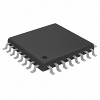
MAX1498ECJ+ Maxim Integrated Products, MAX1498ECJ+ Datasheet - Page 12

MAX1498ECJ+
Manufacturer Part Number
MAX1498ECJ+
Description
IC ADC 4 1/2DIG W/LED DVR 32TQFP
Manufacturer
Maxim Integrated Products
Datasheet
1.MAX1496EAI.pdf
(24 pages)
Specifications of MAX1498ECJ+
Number Of Bits
4.5 Digit
Sampling Rate (per Second)
5
Number Of Converters
1
Power Dissipation (max)
1.65W
Voltage Supply Source
Analog and Digital
Operating Temperature
-40°C ~ 85°C
Mounting Type
Surface Mount
Package / Case
32-LQFP
Lead Free Status / RoHS Status
Lead free / RoHS Compliant
Figure 2 shows the filter frequency response. The
SINC
times the first notch frequency (5Hz). The oversampling
ratio (OSR) for the MAX1496 is 128 and the OSR for the
MAX1447/MAX1498 is 1024.
The output data rate for the digital filter corresponds to
the positioning of the first notch of the filter’s frequency
response. The notches of the SINC
at multiples of the first notch frequency. The SINC
provides an attenuation of better than 100dB at these
notches. For example, 50Hz is equal to 10 times the
first notch frequency and 60Hz is equal to 12 times the
first notch frequency.
For large step changes at the input, allow a settling
time of 800ms before valid data is read.
The MAX1447/MAX1496/MAX1498 contain an internal
oscillator. Using the internal oscillator saves board
space by removing the need for an external clock
source. The oscillator is optimized to give 50Hz and
60Hz power-supply and common-mode rejection.
The MAX1447/MAX1496/MAX1498 contain an internal
charge pump to provide the negative supply voltage
for the internal analog input/reference buffers.
3.5- and 4.5-Digit, Single-Chip ADCs
with LED Drivers
Figure 2. Frequency Response of the SINC
and 60Hz)
12
______________________________________________________________________________________
4
characteristic -3dB cutoff frequency is 0.228
-120
-160
-200
-40
-80
0
0
10
20
FREQUENCY (Hz)
30
Filter Characteristics
40
4
4
Internal Clock
Filter (Notch at 50Hz
filter are repeated
Charge Pump
50
60
4
filter
The bipolar input range of the analog input/reference
buffers allows this device to accept negative inputs
with high source impedances. Connect a 0.1µF capac-
itor from VNEG to GND.
The MAX1447/MAX1498 have a 4.5-digit common-cath-
ode display driver, and the MAX1496 has a 3.5-digit
common-cathode display driver. Figures 3 and 4 show
the connection schemes for a standard seven-segment
LED display. The LED update rate is 2.5Hz. The
MAX1447/MAX1496/MAX1498 automatically display the
results of the ADC, if desired (Table 1).
Figure 3. Segment Connection for the MAX1447/MAX1498
(4.5 Digits)
Figure 4. Segment Connection for the MAX1496 (3.5 Digits)
Table 1. LED Priority Table
X = Don’t care.
F
HOLD
DIGIT 4
1
0
0
D
A
G
F
DIGIT 3
D
G
A
C
B
DP
F
E
PEAK
DIGIT 3
B
C
X
1
0
G
D
A
DP
F
E
DIGIT 2
B
C
G
D
DP
A
E
F
Hold value
Peak value
Latest ADC result
B
DIGIT 2
C
A
G
D
DP
DISPLAY VALUES FORM
E
F
C
B
DIGIT 1
DP
A
G
D
F
E
DIGIT 1
C
B
A
G
D
DP
E
F
DIGIT 0
B
C
A
G
DP
D
LED Driver
F
E
DIGIT 0
B
C
A
G
D
DP
B
C
DP


